
Method for arranging solder ball on printed circuit board

A technology of printed circuit boards and solder balls, which is applied in the direction of printed circuits, printed circuit manufacturing, printed circuit components, etc., and can solve the problem of insufficient heat dissipation by opening windows on the surface

Active Publication Date: 2015-07-01
SHENZHEN GONGJIN ELECTRONICS CO LTD
View PDF5 Cites 5 Cited by
  • Summary
  • Abstract
  • Description
  • Claims
  • Application Information

AI Technical Summary

Problems solved by technology

[0003] However, for printed circuit boards with large heat generation, the heat dissipation of the surface window is still not enough

Method used


Image

  • Method for arranging solder ball on printed circuit board
  • Method for arranging solder ball on printed circuit board

Examples


Embodiment Construction

[0016] In order to make the objects, features and advantages of the present invention more comprehensible, specific implementations of the present invention will be described in detail below in conjunction with the accompanying drawings.

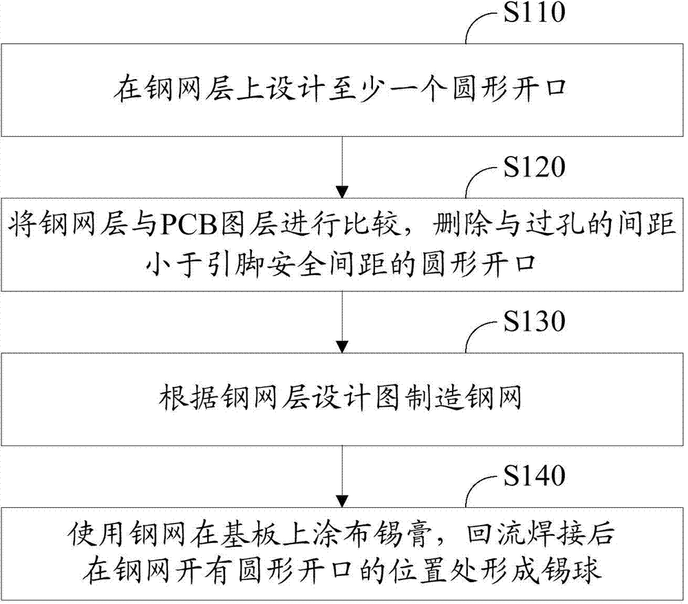
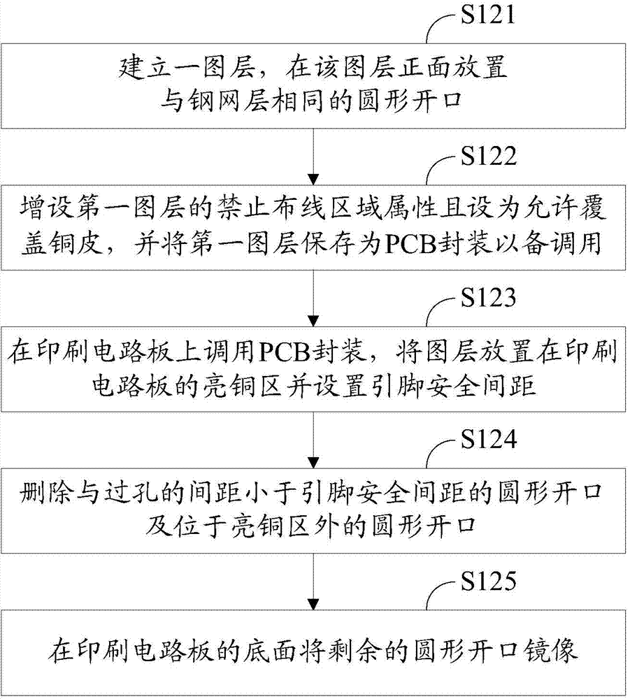
[0017] The invention arranges solder balls at proper positions on the surface of the printed circuit board (PCB), and utilizes the good thermal conductivity of the solder balls to enhance the heat dissipation of the printed circuit board. figure 1 It is a flowchart of a method for setting solder balls on a printed circuit board in an embodiment, including:

[0018] S110, designing at least one circular opening on the steel mesh layer.

[0019] In the manufacturing process of printed circuit boards, solder paste (paste) needs to be coated on at least one side of the PCB, and the stencil will cover the PCB when the solder paste is coated, so the shape and size of the tin formed on the PCB are Determined by the opening of the steel mesh.

[0...


PUM


Abstract

The invention discloses a method for arranging a solder ball on a printed circuit board. The method for arranging the solder ball on the printed circuit board includes that step A, designing at least one round opening in a steel mesh layer; step B, comparing the steel mesh layer with a printed circuit board pattern layer with a hole, and deleting the round openings which are overlapped with the hole or away from the hole by the clearance smaller than a pin safety clearance; C, manufacturing a steel mesh according to a steel mesh layer design drawing of the step B; step D, using the steel mesh to coat solder paste on a substrate, and forming the solder ball at the round opening position of the steel mesh after performing reflow soldering. The method for arranging the solder ball on the printed circuit board can form the solder ball for cooling, the cost is low, the operation is easy to perform, and the method is realized through opening a window on the steel mesh. Through comparing with the hole in the PCB board and deleting the round openings which are overlapped with the hole or away from the hole by the clearance smaller than the pin safety clearance, the solder ball forming at the hole is avoided, and the solder leakage phenomenon can be avoided.

Description

technical field [0001] The invention relates to the field of printed circuits, in particular to a method for arranging solder balls on a printed circuit board. Background technique [0002] For multi-layer printed circuit board (PCB) design, such as four-layer board (signal / ground / power / signal), when there are multiple heat sources (such as DC-DC, AP, etc.), it is necessary to Design the heat dissipation structure of the board, such as opening windows on the surface. [0003] However, for printed circuit boards with large heat generation, the heat dissipation of the surface windows is still not enough. Contents of the invention [0004] Based on this, in order to solve the heat dissipation problem, it is necessary to provide a method for disposing solder balls on the printed circuit board. [0005] A method for setting solder balls on a printed circuit board, comprising the following steps: step A, designing at least one circular opening on the stencil layer; step B, con...

Claims


Application Information

Patent Timeline
IPC IPC(8): H05K1/02
CPCH05K3/0005H05K3/1216
Inventor 谷晓亮
Owner SHENZHEN GONGJIN ELECTRONICS CO LTD
Learn More