
A method for bonding crystal rods

A bonding method and crystal rod technology, which is applied to fine working devices, stone processing equipment, manufacturing tools, etc., can solve the problem of damage to the bonding surface of crystal rods, impact on the bonding surface of silicon rods, uneven force on steel wires, etc. Problems, achieve the effect of reducing damage, ensuring bonding strength, and simple bonding method

Active Publication Date: 2017-04-05
JIANGXI SAI WEI LDK SOLAR HI TECH CO LTD
View PDF6 Cites 0 Cited by
  • Summary
  • Abstract
  • Description
  • Claims
  • Application Information

AI Technical Summary

Problems solved by technology

[0003] However, during ingot gluing, the glue shrinks and releases heat as it cures
Because the glue layer is located between the ingot and the carrier plate, the mechanical stress caused by the shrinkage of the glue and the thermal stress caused by the heat release cannot be released, and the stress will act on the bonding surface of the silicon rod, causing damage to the bonding surface of the ingot and causing silicon In addition, the gas generated when the glue is solidified cannot escape into the air, and pores will be formed in the glue layer, forming the phenomenon of empty glue. When the steel wire cuts the silicon rod to the empty glue position, the steel wire Uneven stress produces abnormal vibration, which will cause abnormal impact on the bonding surface of the silicon rod, resulting in a large number of edge chipping after the completion of the silicon rod slicing.

Method used


Image

  • A method for bonding crystal rods
  • A method for bonding crystal rods
  • A method for bonding crystal rods

Examples


Embodiment 1

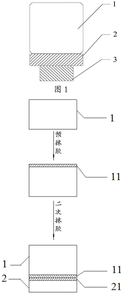
[0044] See attached figure 2 , a method for bonding crystal rods, comprising the following steps:

[0045] (1) Take the polycrystalline silicon rod as the crystal rod to be glued, clean the surface of the crystal rod to be bonded, and then apply glue for pre-applying glue, and form a uniform pre-applying glue layer after the glue is completely cured for 40 minutes. The thickness of the adhesive layer is 100 μm; then the pre-applied adhesive layer is roughened, and the roughened treatment is to use manual sandpaper to polish the pre-applied adhesive layer;

[0046](2) Take the carrier board, apply Wanda wd3640 two-component AB glue on the surface of the carrier board to be bonded, and bond the ingot with the pre-applied glue layer described in step (1) to the carrier board, and wait for the glue to cure After 4 hours, a secondary glue layer is formed to complete the bonding of the ingot.

[0047] Among them, the structure of the polycrystalline rod to be glued is as follows: ...

Embodiment 2

[0056] The technical scheme by embodiment 1 is basically the same, and the difference is that the thickness of the pre-applied adhesive layer is 120 μm, and in step (1), the curing time of glue is 45min, and in step (2), the curing time of glue is 6h, the total thickness of the pre-smear layer and the second-smear layer is 250 μm.

[0057] Cutting the bonded ingot obtained in Example 2, the chipping rate of the obtained silicon wafer was 4.9%, and the hidden cracking rate was 0.5%.

Embodiment 3

[0059] Get the monocrystalline silicon rod as the crystal rod to be glued, and glue the crystal rod according to the technical scheme of Example 1, the difference is that the thickness of the pre-applied glue layer is 80 μm, and in step (1), the glue The curing time is 30 minutes, and in step (2), the curing time of the glue is 6 hours, and the total thickness of the pre-applied glue layer and the second applied glue layer is 200 μm.

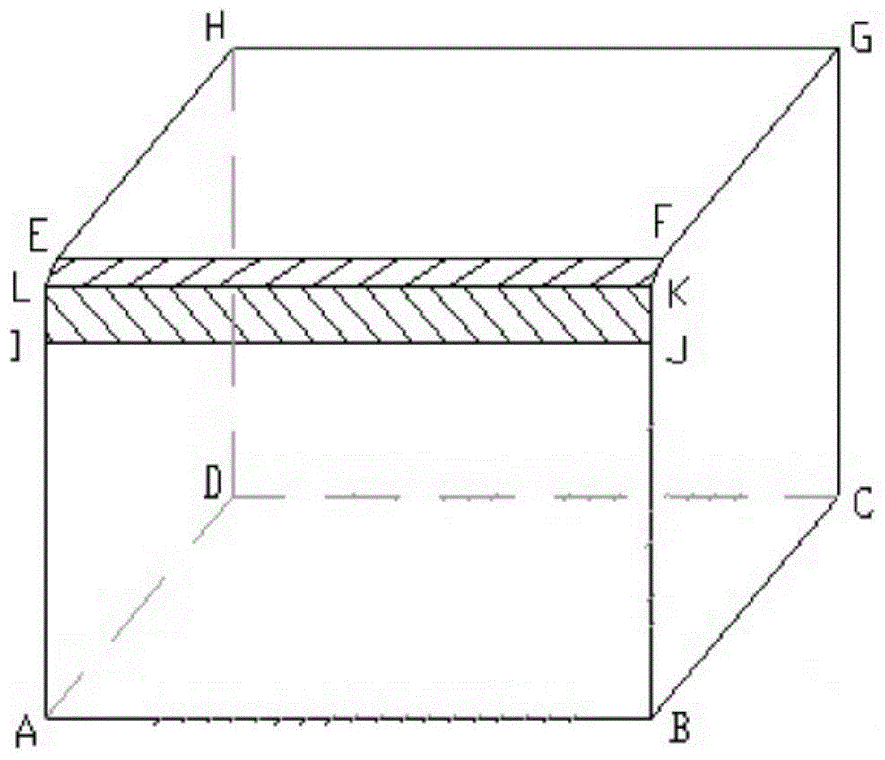
[0060] Among them, the structure of the single crystal ingot to be glued is as follows Figure 5 As shown, the planes ADHE and BCGF are the two end faces of the ingot, the AB direction is the length direction of the ingot, and the BK or AL direction is the direction in which the steel wire cuts the ingot. The plane EFGH is the surface to be bonded between the crystal ingot and the carrier plate, and the plane EFKL is a circular arc chamfering surface, which is parallel to the length direction AB of the crystal ingot. The arc diameter of the circ...


PUM

PropertyMeasurementUnit
thicknessaaaaaaaaaa
thicknessaaaaaaaaaa
thicknessaaaaaaaaaa

Abstract

The invention provides an adhesion method for a crystal bar. The method comprises the steps that before the adhesion of the crystal bar and a bearing plate, adhesives are applied on the crystal bar in advance to form an adhesive layer, and after the adhesive is solidified, adhesion is conducted on the crystal bar with the adhesive layer and the bearing plate by applying the adhesive for a second time. The adhesion method for the crystal bar is simple and efficient, cracks on the adhesive surface of the crystal bar can be reduced, adverse effects caused by the empty adhesive phenomenon are eliminated, the breakage and hidden crack rate in silicon wafer cutting process is further reduced, and the yield of silicon wafers is improved.

Description

technical field [0001] The invention belongs to the technical field of silicon rod cutting, and in particular relates to a method for bonding crystal rods. Background technique [0002] In the manufacturing process of crystalline silicon solar cells, the silicon rods need to be bonded before wire cutting the crystal rods (or silicon rods). The existing method of sticking silicon rods is to first glue the glue board (usually frosted glass) on the supporting board (also known as metal tray, workpiece board, etc.) with glue, and the component obtained after being completely cured is the bearing board; Glue the silicon rod to the adhesive board on the carrier board, and after it is completely cured, fix the bonding assembly (see attached picture 1) formed by the crystal rod, the adhesive board and the supporting board on the wire cutting machine and prepare for cutting . [0003] However, during the ingot gluing process, the glue shrinks and releases heat as it cures. Because...

Claims


Application Information

Patent Timeline
Patent Type & Authority Patents(China)
IPC IPC(8): B28D5/00
CPCB28D5/0082
Inventor 范立峰章金兵宋绍林曹琦
Owner JIANGXI SAI WEI LDK SOLAR HI TECH CO LTD
Learn More