A failure analysis method for ono film defects of flash products
A film defect and failure analysis technology, applied in electrical components, circuits, semiconductor/solid-state device testing/measurement, etc., can solve problems such as indistinguishable, ONO film interference, etc., to improve yield and reliability, and improve efficiency.
- Summary
- Abstract
- Description
- Claims
- Application Information
AI Technical Summary
Problems solved by technology
Method used
Image

Examples
Embodiment Construction
[0023] The specific embodiment of the present invention will be further described in detail below in conjunction with the accompanying drawings.
[0024] It should be noted that, in the following specific embodiments, when describing the embodiments of the present invention in detail, in order to clearly show the structure of the present invention for the convenience of description, the structures in the drawings are not drawn according to the general scale, and are drawn Partial magnification, deformation and simplification are included, therefore, it should be avoided to be interpreted as a limitation of the present invention.
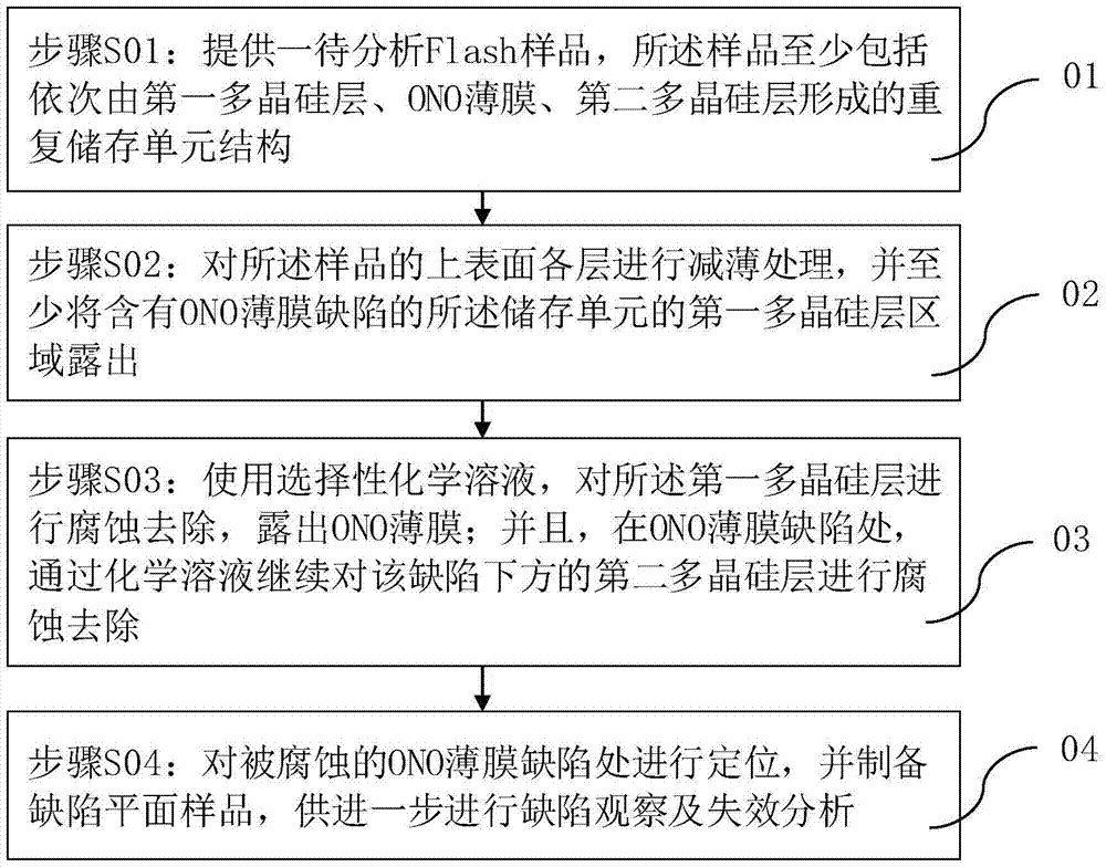
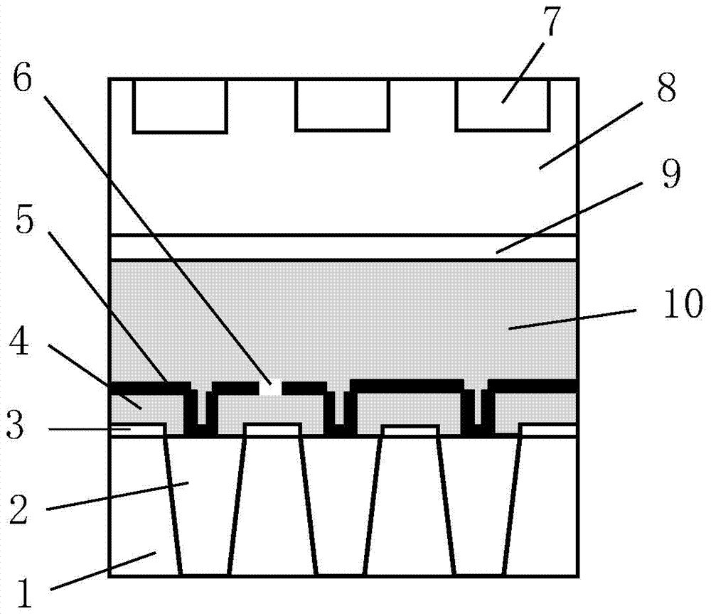
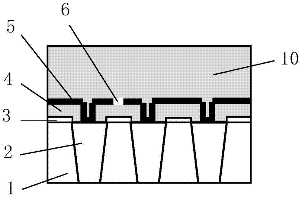
[0025] In the following specific embodiments of the present invention, please refer to figure 1 , figure 1 It is a flow chart of the failure analysis method for the ONO film defect of a Flash product of the present invention; meanwhile, please refer to Figure 2 to Figure 5 as well as Figure 6 ~ Figure 9 ,in, Figure 2 to Figure 5 is used in an ...
PUM
 Abstract
Description
Claims
Application Information
 - R&D Engineer
- R&D Manager
- IP Professional
- Industry Leading Data Capabilities
- Powerful AI technology
- Patent DNA Extraction
Browse by: Latest US Patents, China's latest patents, Technical Efficacy Thesaurus, Application Domain, Technology Topic.
© 2024 PatSnap. All rights reserved.Legal|Privacy policy|Modern Slavery Act Transparency Statement|Sitemap