Method for producing crystalline semiconductor film

A manufacturing method and semiconductor technology, which is applied in semiconductor/solid-state device manufacturing, semiconductor devices, transistors, etc., can solve problems such as component differences and uneven crystallinity, and achieve the effect of reducing the difference in transistor characteristics and effective laser annealing treatment

Active Publication Date: 2018-06-19
JSW阿克迪纳系统有限公司
View PDF6 Cites 0 Cited by
  • Summary
  • Abstract
  • Description
  • Claims
  • Application Information

AI Technical Summary

Problems solved by technology

The problem to be solved in Patent Document 1 is that the sequential scanning of the laser is accompanied by non-uniformity (error) in crystallinity, which causes variation between elements

Method used


Image

  • Method for producing crystalline semiconductor film
  • Method for producing crystalline semiconductor film
  • Method for producing crystalline semiconductor film

Examples


Embodiment 1

[0059] One embodiment of the present invention is described below.

[0060] Using 50 nm-thick amorphous Si as a non-single crystal semiconductor film, pulsed laser irradiation was performed by changing the number of times of irradiation under the following conditions.

[0061] Excimer laser: LSX315C / wavelength 308nm, frequency 300Hz

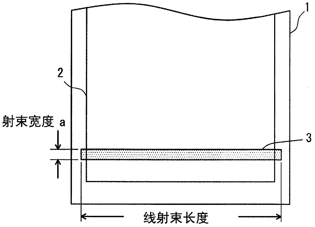
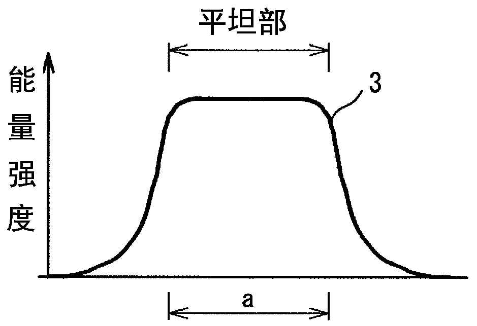
[0062] Beam size: beam length 500mm × beam width 0.16mm

[0063] The beam width is the flat portion in the high-intensity region where the maximum energy intensity is 96% or more

[0064] Scanning pitch: 40μm~80μm

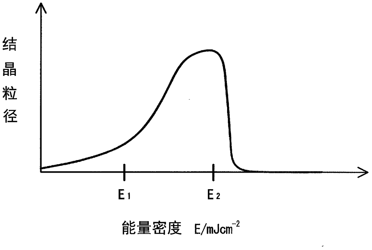
[0065] Irradiation pulse energy density: 370mJ / cm 2

[0066] Channel length: 20μm

[0067] The irradiation pulse energy density of the above-mentioned pulsed laser is below the irradiation pulse energy density capable of producing microcrystals, and within the range of irradiation times from four times to eight times, the crystal grain size gradually grows, and when the number of times of irradiation exceeds eight times When , t...


PUM


Abstract

A manufacturing method in which, when laser-annealing a non-single-crystal semiconductor film, in order to crystallize the semiconductor film using an appropriate scanning pitch and number of irradiation cycles, a line-beam-shaped pulse laser, having a short-axis width of 100-500 µm and a flat section in the beam cross-section shape in the short-axis direction, is scanned relative to the non-single-crystal semiconductor film, whereby the laser moves at each pulse, and performs overlapping irradiation at an irradiation cycle (n), the transistor channel length being defined as b; the pulse laser having an irradiation pulse energy density (E) at which crystal particle size growth reaches saturation due to multiple-cycle irradiation, the density being lower than the irradiation pulse energy density at which microcrystallization occurs on the non-single-crystal semiconductor film due to the irradiation of the pulse laser; the number of irradiation cycles (n) being at least (n0-1), where n0 is the number of irradiation cycles at which the growth in the crystal grain diameter, induced by the pulse laser irradiation having irradiation pulse energy density (E), reaches saturation; the scanning direction of the pulse laser being defined as the channel length direction of the transistor; and a movement amount (c) for each pulse being less than b.

Description

technical field [0001] The present invention relates to a method for producing a crystalline semiconductor film that irradiates a non-single crystal semiconductor film multiple times while moving a pulsed laser beam in the shape of a line beam (overlapping irradiation). Background technique [0002] Generally, thin film transistors used in televisions and computer monitors are made of amorphous silicon (hereinafter referred to as a-silicon), but if silicon is crystallized by a certain method (hereinafter referred to as p-silicon), The function of TFT can be greatly improved. At present, excimer laser annealing technology has been put into practical use as a low-temperature Si crystallization process, and it is widely used for small displays such as mobile phones, and even large-screen displays. [0003] This laser annealing method is to irradiate a non-single crystal semiconductor film with an excimer laser with high pulse energy, thereby making the semiconductor absorbing ...

Claims


Application Information

Patent Timeline
Patent Type & Authority Patents(China)
IPC IPC(8): H01L21/20H01L21/336H01L29/786
CPCH01L21/02532H01L21/02678H01L21/02686H01L21/02691H01L27/1285
Inventor 次田纯一泽井美喜町田政志郑石焕
Owner JSW阿克迪纳系统有限公司
Why Eureka
Try Eureka