Semiconductor imaging device and manufacturing method thereof

A technology of imaging device and manufacturing method, which is applied in semiconductor/solid-state device manufacturing, semiconductor devices, semiconductor/solid-state device components, etc., can solve the problem that it is difficult to obtain semiconductor imaging devices, and achieve the effect of reducing characteristic differences

Inactive Publication Date: 2014-10-22
KK TOSHIBA
View PDF3 Cites 0 Cited by
  • Summary
  • Abstract
  • Description
  • Claims
  • Application Information

AI Technical Summary

Problems solved by technology

[0005] In this way, in the past, there was a characteristic difference between the pixel area and the non-pixel area, and it was difficult to obtain a good semiconductor imaging device.

Method used


Image

  • Semiconductor imaging device and manufacturing method thereof
  • Semiconductor imaging device and manufacturing method thereof
  • Semiconductor imaging device and manufacturing method thereof

Examples


Embodiment Construction

[0017] Embodiments will be described below with reference to the drawings.

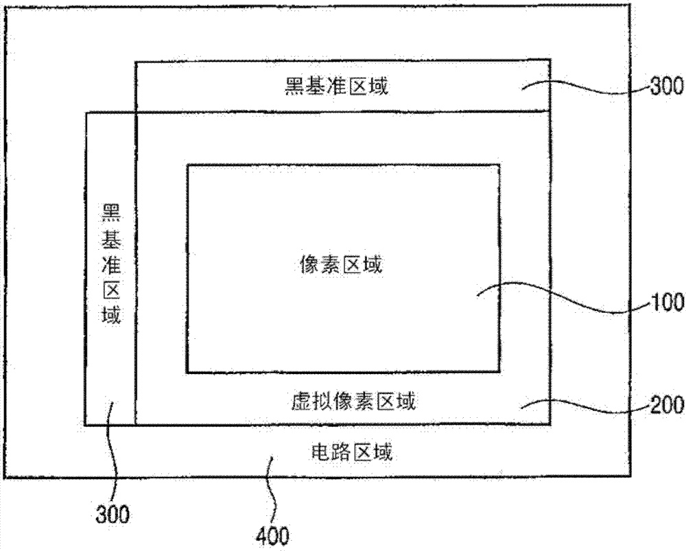
[0018] figure 1 It is a diagram schematically showing the overall configuration of the semiconductor imaging device (CMOS image sensor) according to the embodiment.

[0019] Such as figure 1 As shown, the semiconductor imaging device includes a pixel area 100 , a dummy pixel (Dummy Pixel) area 200 , a black reference area 300 and a circuit area 400 .

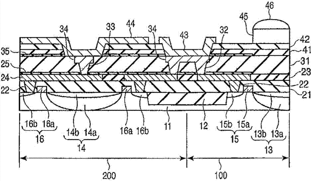
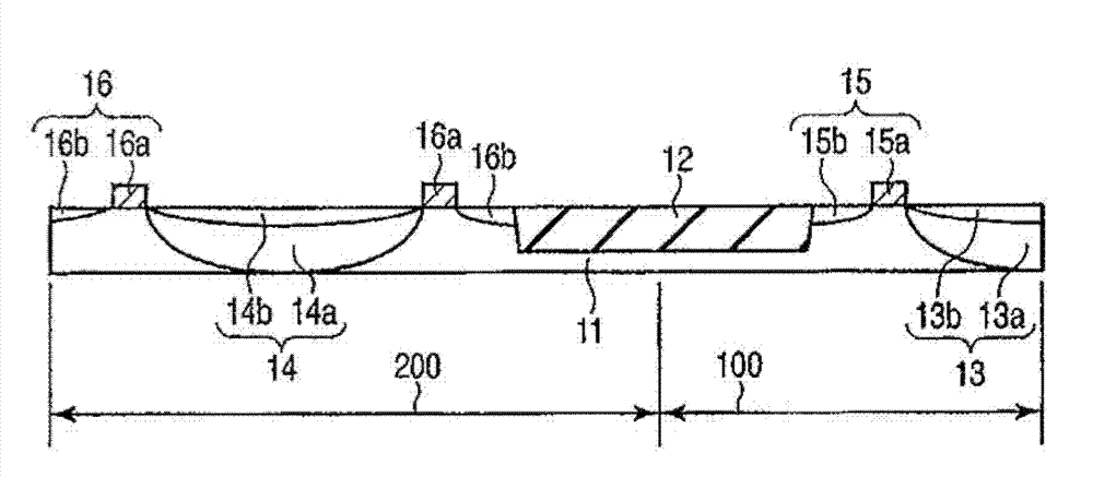
[0020] In the pixel area 100, a plurality of pixels are arranged in a matrix. In each pixel, a photodiode (photoelectric conversion element) and a MOS transistor are provided. A dummy pixel region 200 is arranged around the pixel region 100 . The dummy pixel region 200 is not used in the actual imaging operation, but is provided due to requirements in the manufacturing process and the like. The black reference area 300 is an area where a black reference signal is generated. In non-pixel regions such as the dummy pixel region 200 and the black refe...


PUM


Abstract

According to one embodiment, a semiconductor image pickup device includes a pixel area and a non-pixel area. The device includes a first photoelectric conversion element formed in the pixel area, a first transistor formed in the pixel area and connected to the first photoelectric conversion element, a second photoelectric conversion element formed in the non-pixel area, a second transistor formed in the non-pixel area and connected to the second photoelectric conversion element, a metal wire formed at least in the non-pixel area, a first cap layer formed on the metal wire to prevent diffusion of metal contained in the metal wire, and a dummy via wire formed in the non-pixel area and penetrating the first cap layer.

Description

[0001] This application is based on and claims the priority of Japanese Patent Application No. 2010-251801 filed on November 10, 2010, the entire content of which is incorporated herein. technical field [0002] The present invention relates to a semiconductor imaging device and a manufacturing method thereof. Background technique [0003] In semiconductor imaging devices such as CMOS image sensors, miniaturization is progressing, and copper (Cu) wiring is generally used. In the case of using copper wiring, it is necessary to provide a cover layer such as a silicon nitride film on the copper wiring in order to prevent diffusion of copper. [0004] However, in the pixel region, the cover layer above the photoelectric conversion element is removed in order to suppress attenuation of light incident on the photoelectric conversion element. On the other hand, in non-pixel areas such as dummy pixel areas and black reference areas, the attenuation of light does not need to be supp...

Claims


Application Information

Patent Timeline
Patent Type & Authority Patents(China)
IPC IPC(8): H01L27/146
CPCH01L27/14636H01L27/14623H01L27/14627H01L27/14621H01L27/14643H01L27/14689H01L21/76829H01L23/53228H01L23/53238H01L27/14612H01L27/1463H01L2924/0002
Inventor 小池英敏
Owner KK TOSHIBA
Why Eureka
Try Eureka