
semiconductor memory device

A technology of memory devices and semiconductors, which is applied in the direction of semiconductor devices, semiconductor/solid-state device manufacturing, transistors, etc., can solve the problem of increasing the area of ​​memory arrays, and achieve the effect of reducing the difference in characteristics

Active Publication Date: 2016-08-31
ROHM CO LTD
View PDF3 Cites 0 Cited by
  • Summary
  • Abstract
  • Description
  • Claims
  • Application Information

AI Technical Summary

Problems solved by technology

[0003] However, in the semiconductor memory device of the prior art described above, since the dummy blocks D1 and D2 having the same size as the element block A are provided, there is a problem that the area of ​​the memory array is increased unnecessarily.
especially if Figure 13 As shown, in the case where the memory array is divided into multiple pieces and arranged, the formation area of ​​the dummy blocks D1 and D2 increases with the increase of the end portion of the memory array, so the above-mentioned problem becomes particularly prominent.

Method used


Image

  • semiconductor memory device
  • semiconductor memory device
  • semiconductor memory device

Examples


Embodiment Construction

[0026] Various embodiments are now described with reference to the drawings, wherein like symbols are used to refer to like elements throughout. In the following description, for purposes of explanation, numerous specific details are set forth in order to provide a thorough understanding of one or more embodiments. It is evident, however, that such embodiments may be practiced without these specific details. In other instances, well-known structures and devices are shown in block diagram form to facilitate the description of one or more embodiments.

[0027] 【Block Diagram

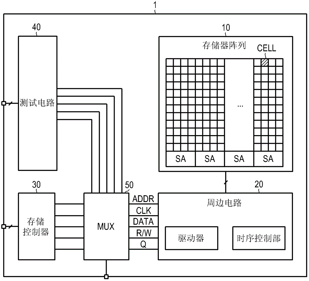
[0028] figure 1 is a block diagram showing an embodiment of the semiconductor memory device of the present invention. The semiconductor memory device of this embodiment includes a memory array 10 , a peripheral circuit 20 , a memory controller 30 , a test circuit 40 and a multiplexer 50 .

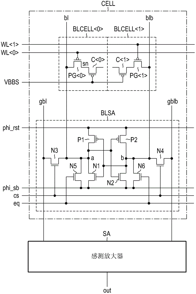
[0029] The memory array 10 includes a plurality of memory cells CELL and sense amplifiers SA arranged in an arr...


PUM


Abstract

The invention discloses a semiconductor memory device, which comprises: a memory array containing a plurality of element blocks, the plurality of element blocks include a terminal element block arranged at the terminal part of the memory array; and adjacent to the terminal element block , but at least one virtual block that is not actually used; wherein, the layout pattern of the at least one virtual block only corresponds to a part of the layout patterns of the plurality of element blocks.

Description

technical field [0001] The present invention relates to a pattern design of a semiconductor memory device including a memory-mounted LSI (Large Scale Integrated Circuit). Background technique [0002] Figure 12 It is a schematic diagram showing a layout pattern (Layout pattern) of a conventional memory array (Memory array) terminal portion. Such as Figure 12 As shown, in the semiconductor memory device of the prior art, in order to place an element block A (for forming memory cells, sense amplifiers, etc. Transistor group) and element block B (transistor group used to form memory cells, sense amplifiers, etc., as in element block A) not arranged at the end of the memory array, there is no difference in density of the mask pattern (further In other words, the resulting difference in characteristics), while the adjacent element block A is provided with virtual blocks D1 and D2 that are not actually used. [0003] However, in the conventional semiconductor memory device des...

Claims


Application Information

Patent Timeline
Patent Type & Authority Patents(China)
IPC IPC(8): H01L27/108G11C11/4063G11C11/413H10B12/00H10B10/00
CPCG11C11/4099G11C11/412G11C29/1201H01L27/0207G11C5/025H10B12/09H10B12/50H10B10/12H10B10/18H01L21/82G11C7/06G11C7/14
Inventor 鹈饲和久
Owner ROHM CO LTD
Learn More