
MEMS sensing chip

一种传感芯片、芯片的技术,应用在MEMS传感芯片领域,能够解决管壳破裂、封装可靠性差、固有频率低等问题,达到降低切割和打线的难度、防护机械性损毁、灵敏性提高的效果

Active Publication Date: 2015-09-02
MIRAMEMS SENSING TECH CO LTD
View PDF5 Cites 0 Cited by
  • Summary
  • Abstract
  • Description
  • Claims
  • Application Information

AI Technical Summary

Problems solved by technology

Practice has shown that the existing sensor packaging technology generally has the problems of poor resistance to high overload, low natural frequency, and poor packaging reliability. , there are often problems such as shell cracking, cover plate depression, chip falling off from the shell substrate, lead wire breakage, etc.

Method used


Image

  • MEMS sensing chip
  • MEMS sensing chip
  • MEMS sensing chip

Examples


Embodiment

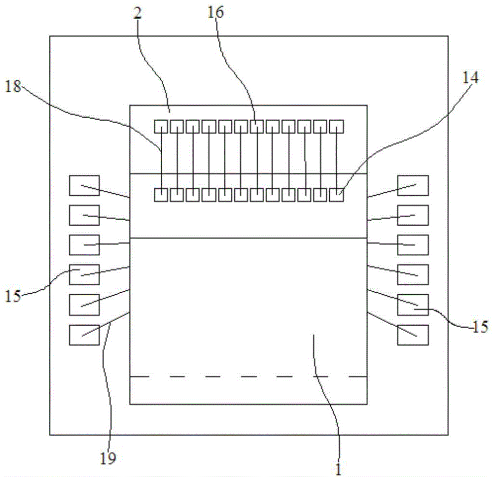
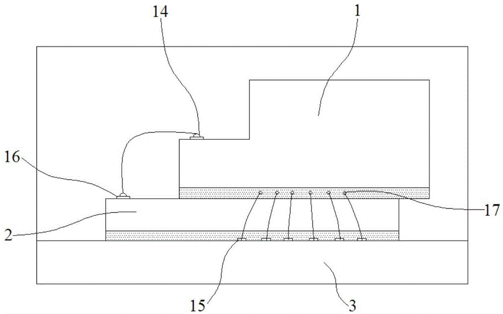
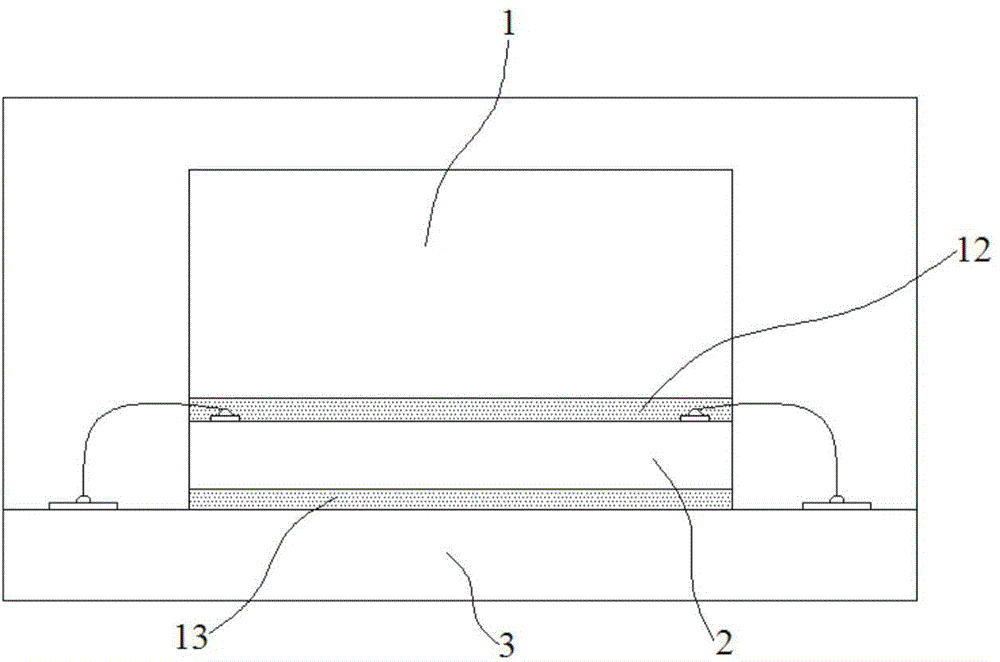
[0028] Embodiment: a kind of MEMS sensing chip, comprises MEMS acceleration chip 1, is used for filtering the signal processing chip 2 of interference signal and processing induction signal and substrate 3, described MEMS acceleration chip 1 is made up of cover body 4, micromechanical system 5 and A circuit substrate 6 for generating induction signals. The micromechanical system 5 is composed of an X-axis acceleration sensing area 7, a Y-axis acceleration sensing area 8, and a Z-axis acceleration sensing area 9 for sensing external Z-axis motion. The cover Body 4 and circuit substrate 6 are bonded by a sealant layer 10 to form a sealed cavity 11. The micromechanical system 5 is located in the sealed cavity 11 and on the upper surface of the circuit substrate 6. The height of the sealed cavity 11 is 45~55μm;

[0029] The X-axis acceleration sensing area 7 includes an X-direction "H"-shaped moving piece 71 with two through holes, two X-direction moving electrodes 72 and two X-di...


PUM


Abstract

A capacitive MEMS acceleration sensor comprising an MEMS acceleration chip (1), a signal processing chip (2) and a substrate (3). The MEMS acceleration chip (1) comprises a cover body (4), a micromechanical system (5) and a circuit substrate (6), the micromechanical system (5) is composed of an X-axis acceleration induction area (7), a Y-axis acceleration induction area (8) and a Z-axis acceleration induction area (9); the Y-axis acceleration induction area (8) comprises a Y-direction 'H'-shaped moving sheet (81) with two through holes, two Y-direction moving electrodes (82) and two Y-direction fixed electrodes (83); the Z-axis acceleration induction area (9) comprises a mass block (24) and a supporting shaft (25) for supporting the center of the mass block (24); the lower surface of the circuit substrate (6) is bonded with a partial area on the upper surface of the signal processing chip (2) through a first insulation adhesive layer (12); the upper surface of the circuit substrate (6) is provided with a plurality of chip welding points (14), the upper surface of the substrate (3) is provided with a plurality of substrate welding points (15) which are distributed in the edge areas on the two sides of the substrate (3), and the upper surface of the signal processing chip (2) is provided with signal input welding points (16) and signal output welding points (17) respectively. The capacitive MEMS acceleration sensor improves the reliability of a device and effectively reduces stress damage to the chips by an external force.

Description

technical field [0001] The invention relates to the technical field of acceleration sensors, in particular to a MEMS sensor chip. Background technique [0002] The research on acceleration sensors has developed rapidly in recent years, and high-range acceleration sensors with various performances and ranges have been reported one after another. However, the accelerometer has high requirements for high overload resistance and natural frequency. Usually, the high overload resistance is required to withstand hundreds of thousands of range impact loads, and the natural frequency is required to be as high as tens of kHz, or even hundreds of kHz. Therefore, in applications, MEMS high-range acceleration sensors often lead to structural failure due to their poor ability to withstand high overloads. In order to ensure the reliability of the MEMS high-range acceleration sensor in application, the packaging of the MEMS high-range acceleration sensor is particularly important. Practic...

Claims


Application Information

Patent Timeline
Patent Type & Authority Applications(China)
IPC IPC(8): G01P15/18
CPCG01P15/125G01P15/18G01P2015/0831
Inventor 陈学峰钟利强杨小平
Owner MIRAMEMS SENSING TECH CO LTD
Learn More