Image processing apparatus and method for controlling image processing apparatus
An image processing device and image technology, applied in the direction of image communication, color TV parts, TV system parts, etc., can solve the problem that the angle of the subject cannot be detected correctly
- Summary
- Abstract
- Description
- Claims
- Application Information
AI Technical Summary
Problems solved by technology
Method used
Image

Examples
no. 1 example
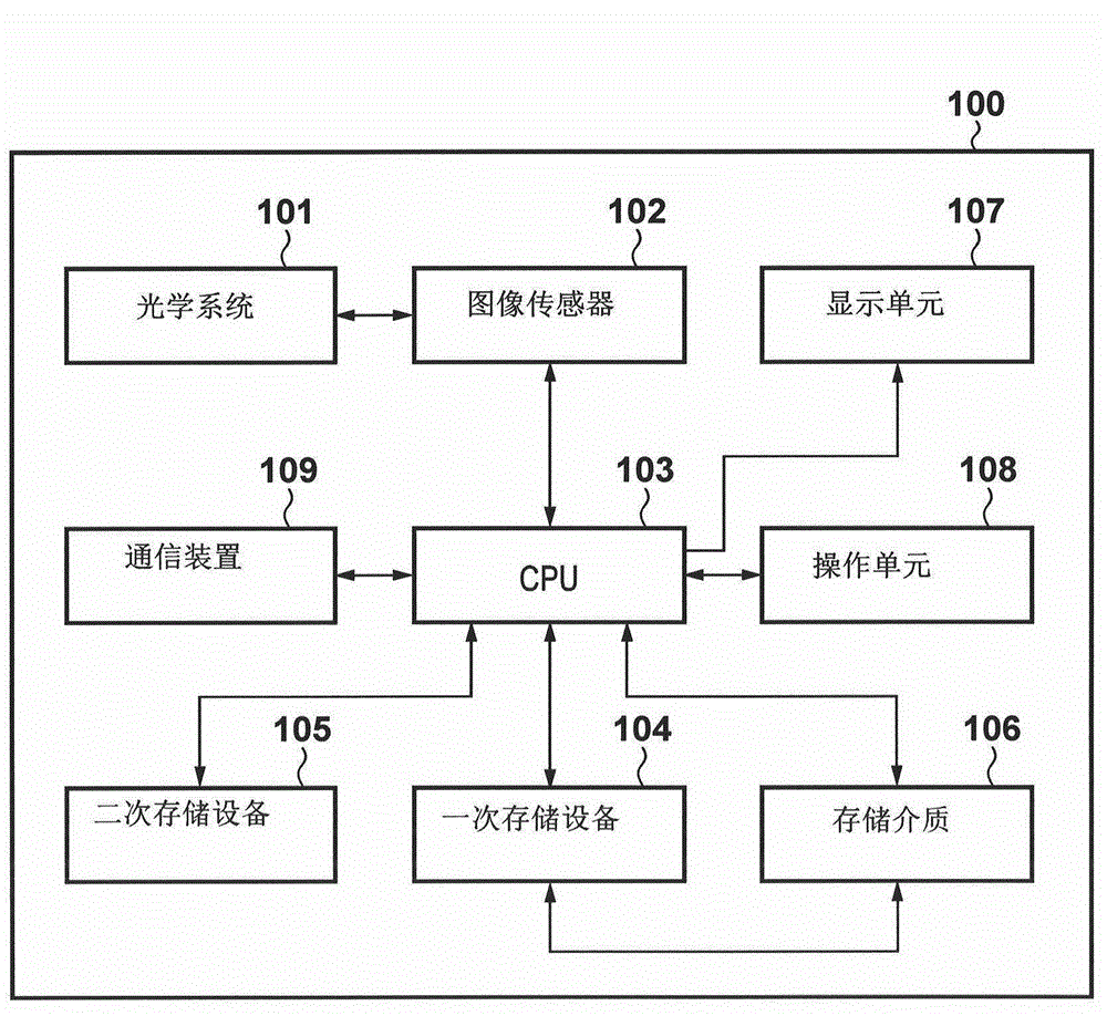
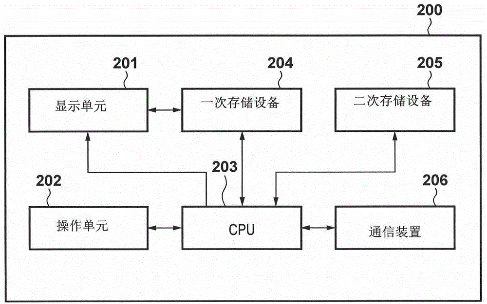
[0029] Figure 1A is a block diagram showing an exemplary functional configuration of an imaging device (or image processing device) 100 as an exemplary image processing device according to an embodiment of the present invention.
[0030] The imaging device 100 is a device such as a digital still camera or a digital video camera that captures a subject and obtains data (image data) representing an image of the subject. The optical system 101 has a lens, a shutter, and a diaphragm, and forms an optical image of a subject on an image sensor 102 under the control of a CPU 103 . The image sensor 102 , which may be a CCD or a CMOS image sensor, performs photoelectric conversion at each pixel on a formed optical image of a subject, and converts it into an analog image signal. The CPU 103 converts an analog image signal into a digital image signal (image data), and applies it to so-called development processing and encoding processing such as white balance adjustment and color inter...
no. 2 example
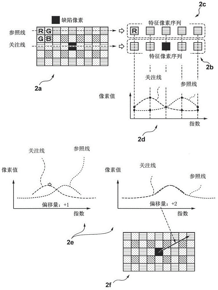
[0066] The first embodiment describes a correction method in a case where a defective pixel is a pixel of a color that appears once in each repeating unit of a color filter, such as an R pixel or a B pixel in a Bayer array. The present embodiment relates to a correction method in a case where a defective pixel is a pixel present in each pixel line such as a G pixel in a Bayer array.
[0067] In the case where the R pixel or the B pixel in the Bayer array is a defective pixel, since the repeating unit is composed of two pixels, a pixel having the same color as the defective pixel does not exist in an adjacent pixel line but is located at least two pixels away from the defective pixel. pixels, so that the reference line is set on the pixel line separated by two pixels from the line of interest. However, for example, if the G pixel is such as Figure 6 For a defective pixel in part 6a of , a pixel of the same color as the defective pixel exists on an adjacent pixel line. For th...
no. 3 example
[0072] The first and second embodiments describe correction methods in the case where defective pixels are isolated. This embodiment will describe a correction method in the case where defective pixels of the same color continuously exist. Such defective pixels occur due to manufacturing tolerances or deterioration over time, and if Figure 7 As shown in part 7a of , such defective pixels also occur in the case where pixels for focus detection are arranged in an image sensor. Since the focus detection pixels generate signals for performing focus detection in the phase difference detection method, their light-receiving range is narrower than that of normal pixels, or no color filter is provided in them, so the obtained pixel values are different from those of normal pixels. The pixel values are different. Therefore, if Figure 7 As shown in part 7b of , a correction needs to be performed considering that these focus detection pixels will be consecutive defective pixels o...
PUM
 Abstract
Description
Claims
Application Information
 - R&D
- Intellectual Property
- Life Sciences
- Materials
- Tech Scout
- Unparalleled Data Quality
- Higher Quality Content
- 60% Fewer Hallucinations
Browse by: Latest US Patents, China's latest patents, Technical Efficacy Thesaurus, Application Domain, Technology Topic, Popular Technical Reports.
© 2025 PatSnap. All rights reserved.Legal|Privacy policy|Modern Slavery Act Transparency Statement|Sitemap|About US| Contact US: help@patsnap.com