
Monitoring layout and monitoring method of gate process

A gate and process technology, applied in the field of gate process monitoring layout, can solve the problems of process step deviation, low semiconductor production yield, poor reliability of monitoring results, etc., and achieve the effect of high reliability and accuracy

Active Publication Date: 2017-12-01
SEMICON MFG INT (SHANGHAI) CORP
View PDF5 Cites 0 Cited by
  • Summary
  • Abstract
  • Description
  • Claims
  • Application Information

AI Technical Summary

Problems solved by technology

[0005] However, in the prior art, the use of OCD technology to monitor the characteristic dimensions of the gate process has the problem of poor reliability of the monitoring results, and it is difficult to judge whether the gate process meets the process standards and which process step in the gate process has occurred. Deviation, leading to low yield of semiconductor production

Method used


Image

  • Monitoring layout and monitoring method of gate process
  • Monitoring layout and monitoring method of gate process
  • Monitoring layout and monitoring method of gate process

Examples


Embodiment Construction

[0037] It can be seen from the background art that the monitoring reliability of the gate process in the prior art is poor, and it is difficult to judge whether there is a deviation in the gate process, resulting in a low yield rate of semiconductor production.

[0038]The OCD monitoring method for the characteristic size of the gate process is studied. The monitoring of the gate process includes after development inspection (ADI: After Develop Inspection) and after etching inspection (AEI: After Etch Inspection). Among them, post-development inspection refers to It is: after the patterned photoresist is formed, the characteristic size and alignment characteristics of the patterned photoresist are monitored. Post-etching monitoring refers to: after the etching process is completed, the pattern formed by etching Monitoring of feature size and alignment characteristics. Through the analysis of ADI monitoring data and AEI monitoring data, it can be judged whether the gate process...


PUM


Abstract

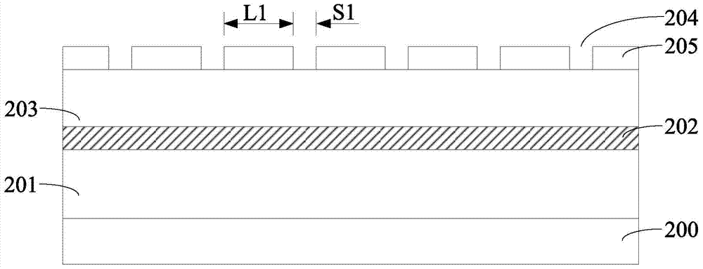
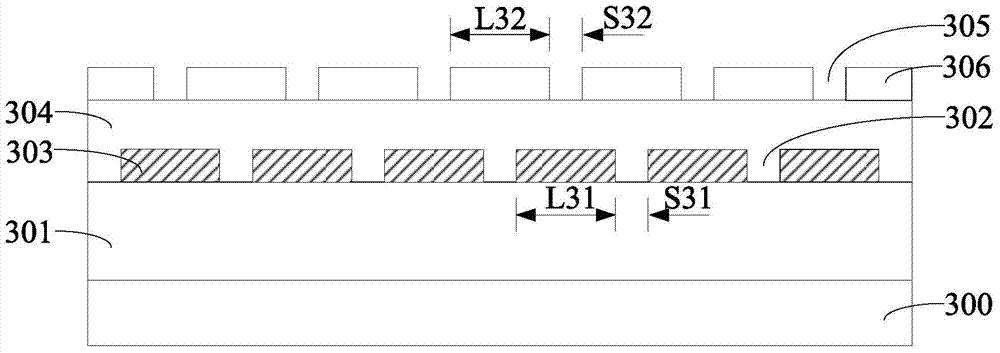
Provided is a gate technology monitoring layout and monitoring method. The gate technology monitoring layout comprises a first monitoring layout and a second monitoring layout. The first monitoring layout comprises a first substrate, a first initial gate; a first mask layer covering the surface of the first initial gate; a first pattern transfer layer covering the surface of the first mask layer; and a first photoresist layer covering the surface of the first pattern transfer layer and provided with a first pattern. The second monitoring layout comprises a second substrate, a second initial gate; a second mask layer arranged on the surface of the second initial gate and provided with a second pattern; a second pattern transfer layer covering the surface of the second mask layer and exposing the surface of the second initial gate; and a second photoresist layer covering the surface of the second pattern transfer layer and provided with a third pattern. The monitoring layout and the monitoring method may acquire an ADI monitored result and an AEI monitored result of gate technology, timely regulate the gate technology according to the ADI monitored result and the AEI monitored result, and improve a semiconductor production yield rate.

Description

technical field [0001] The invention relates to the technology in the field of semiconductor manufacturing, in particular to a monitoring layout and a monitoring method of a gate process. Background technique [0002] Due to the rapid development of integrated circuit technology, it is a common trend to increase the integration of devices. When the integration level of devices continues to increase, the size of devices and the distance between devices will be shortened synchronously. [0003] As the size of devices continues to shrink, the process of forming devices is facing more and more challenges. For example, as the size of devices continues to shrink, it is easy to cause deviations in the gate feature size and alignment characteristics of the formed devices. For example, The tail of the gate is pulled back (shortened) so that the edge of the gate does not fully cover the active area, resulting in a low ability of the device to control the voltage and resulting in a la...

Claims


Application Information

Patent Timeline
Patent Type & Authority Patents(China)
IPC IPC(8): H01L21/66
CPCH01L22/12
Inventor 胡华勇林益世
Owner SEMICON MFG INT (SHANGHAI) CORP
Learn More