Display device, display panel and manufacturing method thereof

A technology for display panels and substrates, which is applied to semiconductor/solid-state device components, semiconductor devices, electrical components, etc., and can solve problems such as display panels and display devices not working properly.

Active Publication Date: 2018-09-28
WUHAN TIANMA MICRO ELECTRONICS CO LTD +1
View PDF9 Cites 0 Cited by
  • Summary
  • Abstract
  • Description
  • Claims
  • Application Information

AI Technical Summary

Problems solved by technology

[0004] In view of this, the present invention provides a display device, a display panel and a manufacturing method thereof, so as to solve the problem in the prior art that the display panel and the display device cannot work normally due to micro-cracks in the encapsulation layer

Method used


Image

  • Display device, display panel and manufacturing method thereof
  • Display device, display panel and manufacturing method thereof
  • Display device, display panel and manufacturing method thereof

Examples


Embodiment Construction

[0030] The following will clearly and completely describe the technical solutions in the embodiments of the present invention with reference to the accompanying drawings in the embodiments of the present invention. Obviously, the described embodiments are only some, not all, embodiments of the present invention. Based on the embodiments of the present invention, all other embodiments obtained by persons of ordinary skill in the art without making creative efforts belong to the protection scope of the present invention.

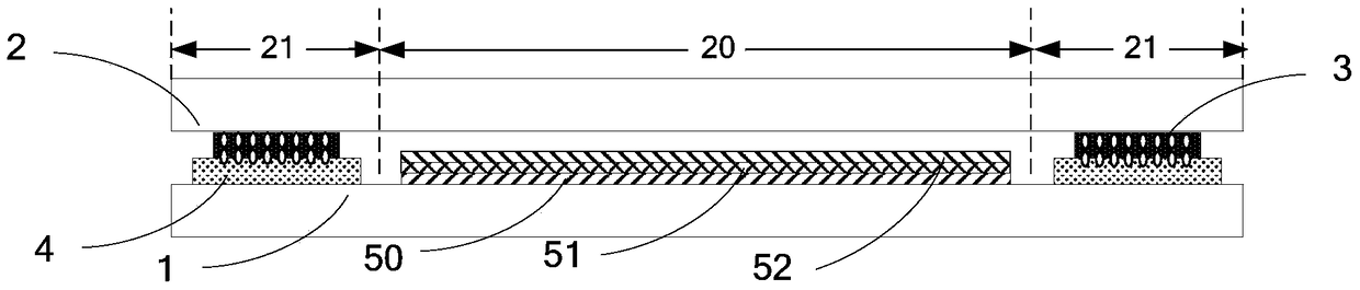
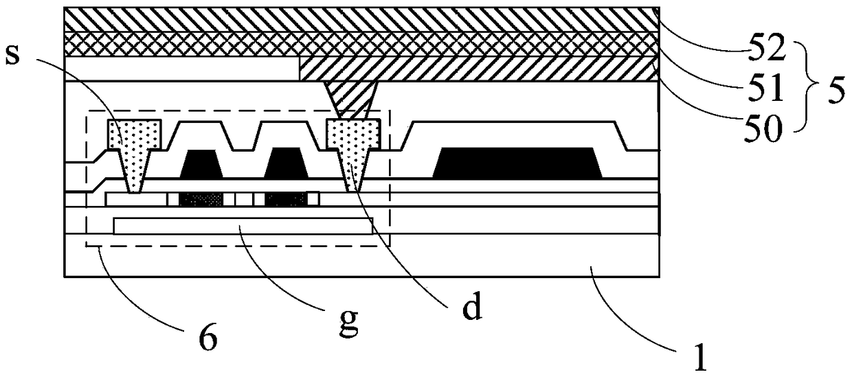
[0031] An embodiment of the present invention provides a display panel. Optionally, the display panel may be an organic light-emitting display panel. Refer to Figure 2a , Figure 2a A schematic cross-sectional structure diagram of the display panel provided in this embodiment.

[0032] The display panel includes a first substrate 1, a second substrate 2 and an encapsulation layer 3 between the first substrate 1 and the second substrate 2, wherein the first s...


PUM


Abstract

The invention provides a display device, a display panel and a manufacturing method thereof. The display panel comprises a first substrate, a second substrate and a packaging layer arranged between the first substrate and the second substrate. The packaging layer is arranged in an edge packaging area of the display panel, and the packaging layer is provided with a plurality of repairing capsules. The repairing capsules are used for releasing glue therein when cracks appear on the packaging layer. The glue dries and seals the cracks after contacting air, so that the problem that the performance of an organic luminescent layer in a packaging box is influenced because oxygen and water vapor in the air enter the internal part of the display panel through the cracks is prevented, and the problems that the display panel fails to work normally or is even scrapped and the service lifetime of the display device is seriously influenced are further solved.

Description

technical field [0001] The present invention relates to the field of display technology, and more specifically, to a display device, a display panel and a manufacturing method thereof. Background technique [0002] refer to figure 1 , figure 1 It is a structural schematic diagram of an existing organic light-emitting display panel. The display device includes a display area 10 and a non-display area 11 located around the display area 10. The non-display area 11 corresponds to a package between the lower substrate and the upper substrate. layer 110, so as to encapsulate the organic light-emitting layer and the like between the upper and lower substrates, so as to prevent air and the like from affecting the light-emitting performance of the organic light-emitting layer. [0003] However, in the process of actual application, the encapsulation layer will have micro-cracks due to internal stress, local aging of materials, and hardening, which will cause air or water vapor to e...

Claims


Application Information

Patent Timeline
Patent Type & Authority Patents(China)
IPC IPC(8): H01L23/28H01L27/32
Inventor 李玉军
Owner WUHAN TIANMA MICRO ELECTRONICS CO LTD
Why Eureka
Try Eureka