A kind of electro-optic crystal thin film, preparation method and electronic component

A technology of electro-optic crystals and thin films, which is applied in the direction of optical components, instruments, light guides, etc., can solve the problems of thin film layer damage and etching processing difficulties, and achieve the effect of improving etching efficiency

Active Publication Date: 2022-05-17
JINAN JINGZHENG ELECTRONICS
View PDF0 Cites 0 Cited by
  • Summary
  • Abstract
  • Description
  • Claims
  • Application Information

AI Technical Summary

Problems solved by technology

[0005] In order to solve the problem in the prior art that the etching process on the thin film layer is very difficult and will cause certain damage to the thin film layer, the application provides an electro-optic crystal thin film, a preparation method and electronic components

Method used


Image

  • A kind of electro-optic crystal thin film, preparation method and electronic component
  • A kind of electro-optic crystal thin film, preparation method and electronic component
  • A kind of electro-optic crystal thin film, preparation method and electronic component

Examples


Embodiment 1

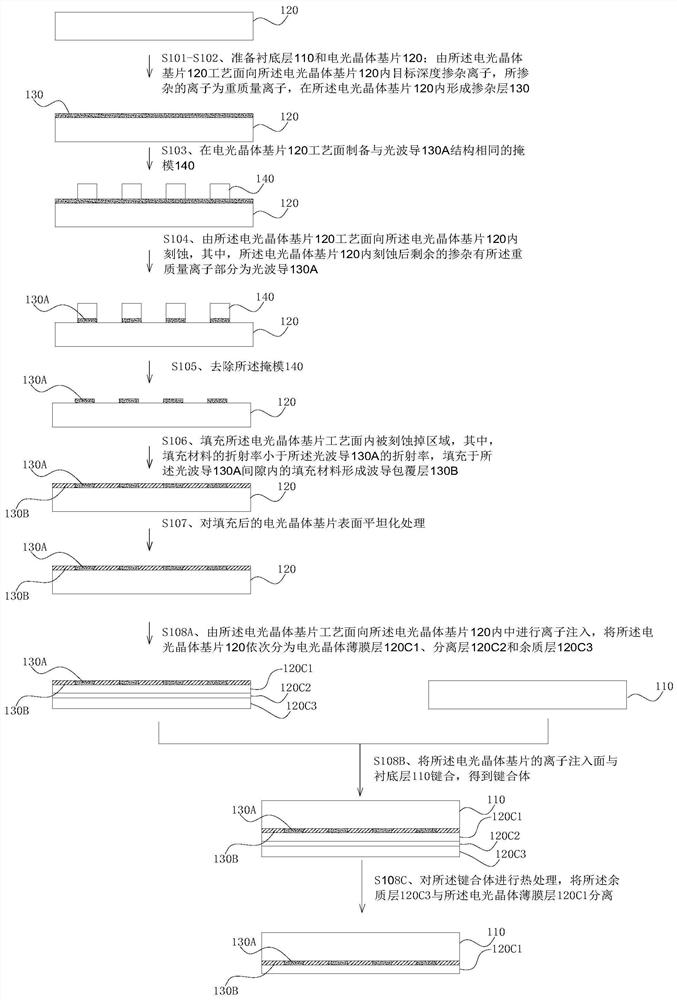
[0033] see figure 1 , Embodiment 1 of the present application provides a method for preparing an electro-optic crystal thin film, comprising the following steps:

[0034] Step 101 , preparing the substrate layer 110 and the electro-optic crystal substrate 120 .

[0035] The substrate layer 110 in the embodiment of the present application may be a single-layer substrate or a composite substrate, which is not limited in the present application, wherein the materials of each substrate in the composite substrate may be the same or different. Applications are not limited to this either. The substrate layer 110 can be made of materials such as lithium niobate, lithium tantalate, quartz, silicon, sapphire, SOI, diamond, silicon carbide, silicon nitride, gallium arsenide, or indium phosphide, which is not limited in this application.

[0036] The electro-optic crystal substrate 120 in the embodiment of the present application refers to the basic material with a certain thickness for p...

Embodiment 2

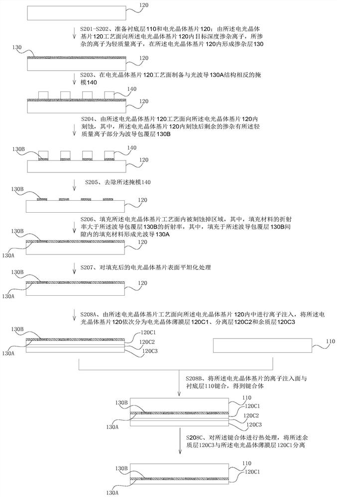
[0095] Embodiment 2 is basically the same as the above-mentioned Embodiment 1, the difference is that the ions doped from the electro-optic crystal substrate process to the target depth in the electro-optic crystal substrate in the embodiment 2 of the present application are light-weight ions. The preparation method provided in Example 2 is described.

[0096] see figure 2 , Embodiment 2 of the present application provides a method for preparing an electro-optic crystal thin film, comprising the following steps:

[0097] Step 201 , preparing the substrate layer 110 and the electro-optic crystal substrate 120 .

[0098]Step 202, using the electro-optic crystal substrate process to deeply dope ions toward the target in the electro-optic crystal substrate, the doped ions are light-weight ions, and form a doped layer 130 in the electro-optic crystal substrate 120, Wherein, the refractive index of the portion of the electro-optic crystal substrate doped with the light-mass ion i...

Embodiment 3

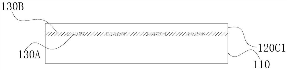
[0114] see image 3 Embodiment 3 of the present application provides an electro-optic crystal thin film, which can be prepared by the preparation method provided in Embodiment 1 above. The prepared electro-optic crystal thin film includes an electro-optic crystal thin film layer 120C1 and a substrate layer 110. The electro-optic crystal thin film layer 120C1 includes a doped region, wherein the doped ions in the doped region are heavy mass ions, the doped region forms an optical waveguide 130A, and the gap of the optical waveguide 130A is filled with a filling material to form a waveguide cladding layer 130B, the top surface of the optical waveguide 130A is on the same level as the top surface of the electro-optic crystal film layer 120C1, wherein the refractive index of the portion doped with the heavy mass ions in the electro-optic crystal film layer 120C1 is greater than that of the electro-optic crystal film layer The layer 120C1 is not doped with the refractive index of t...


PUM

PropertyMeasurementUnit
thicknessaaaaaaaaaa
thicknessaaaaaaaaaa
surface roughnessaaaaaaaaaa

Abstract

The application discloses an electro-optic crystal thin film, a preparation method and electronic components, including: doping heavy mass ions at a target depth in the electro-optic crystal substrate by the process of the electro-optic crystal substrate; preparation and optical waveguide structure on the process surface of the electro-optic crystal substrate The same mask; the electro-optic crystal substrate process faces the electro-optic crystal substrate to be etched, and the remaining part doped with heavy mass ions after etching in the electro-optic crystal substrate is an optical waveguide; the electro-optic crystal substrate process surface is filled with The area is etched away, and the refractive index of the filling material is smaller than that of the optical waveguide, wherein the filling material filled in the gap of the optical waveguide forms a waveguide cladding layer. The electro-optic crystal film substrate is doped to form lattice damage in the electro-optic crystal film substrate, thereby improving the etching efficiency and avoiding the problem that directly etching the electro-optic crystal film substrate will affect the performance of the electro-optic crystal film layer.

Description

technical field [0001] The application belongs to the field of semiconductor element preparation, and in particular relates to an electro-optic crystal thin film, a preparation method and electronic components. Background technique [0002] Electro-optic crystal materials such as lithium niobate or lithium tantalate are widely used in nonlinear optics, ferroelectricity, and piezoelectricity due to their advantages such as high Curie temperature, strong spontaneous polarization, high electromechanical coupling coefficient, and excellent electro-optic effect. , electro-optic and other fields, especially in the fields of thin-film bulk acoustic wave devices, filters, optical modulators, etc., have received more and more attention and applications. If electro-optic crystal materials such as lithium niobate or lithium tantalate are used to prepare optical modulators, the lithium niobate thin film needs to be further prepared into the required optical waveguide structure, and then...

Claims


Application Information

Patent Timeline
Patent Type & Authority Patents(China)
IPC IPC(8): G02F1/035G02F1/03G02B6/136G02B6/134G02B6/13G02B6/12
CPCG02F1/0305G02F1/035G02B6/12G02B6/13G02B6/1347G02B6/136G02B2006/12188G02B2006/12176G02B2006/12173G02B2006/12197Y02P70/50
Inventor 王金翠张秀全刘桂银张涛连坤刘阿龙杨超
Owner JINAN JINGZHENG ELECTRONICS
Why Eureka
Try Eureka