Photolithography method

A photolithography and photoresist technology, applied in the field of photolithography, can solve problems such as difficulty in achieving the expected shape, and the optical diffraction effect cannot be 100% anisotropic.

Active Publication Date: 2016-08-31
SEMICON MFG INT (SHANGHAI) CORP
View PDF6 Cites 0 Cited by
  • Summary
  • Abstract
  • Description
  • Claims
  • Application Information

AI Technical Summary

Problems solved by technology

[0003] In the photolithography process, especially when making small-scale shapes, due to the optical diffraction effect and the etching itself cannot achieve 100% anisotropy, it will be difficult to achieve the desired shape after etching.

Method used


Image

  • Photolithography method
  • Photolithography method
  • Photolithography method

Examples


Embodiment Construction

[0011] The principles and features of the present invention are described below in conjunction with the accompanying drawings, and the examples given are only used to explain the present invention, and are not intended to limit the scope of the present invention.

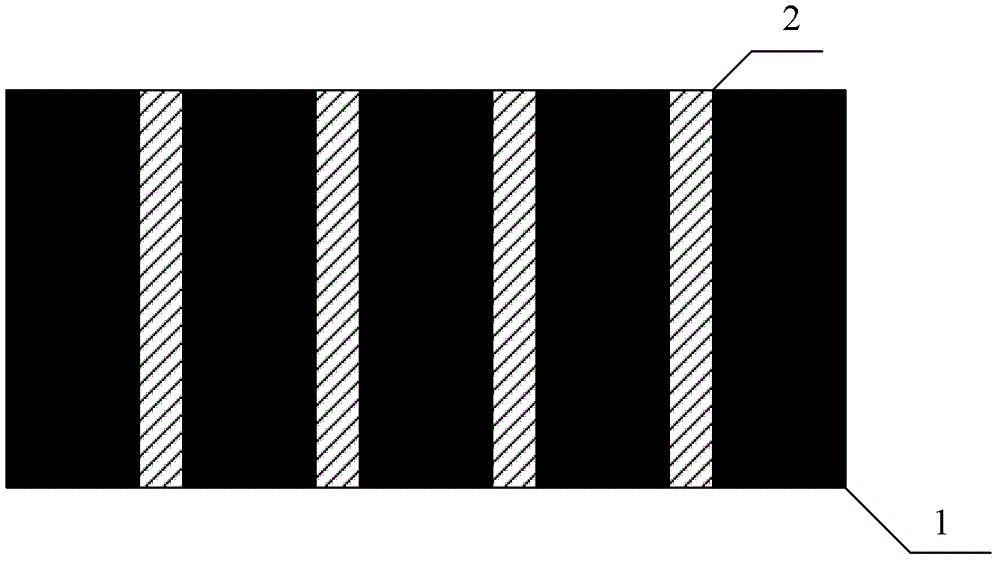
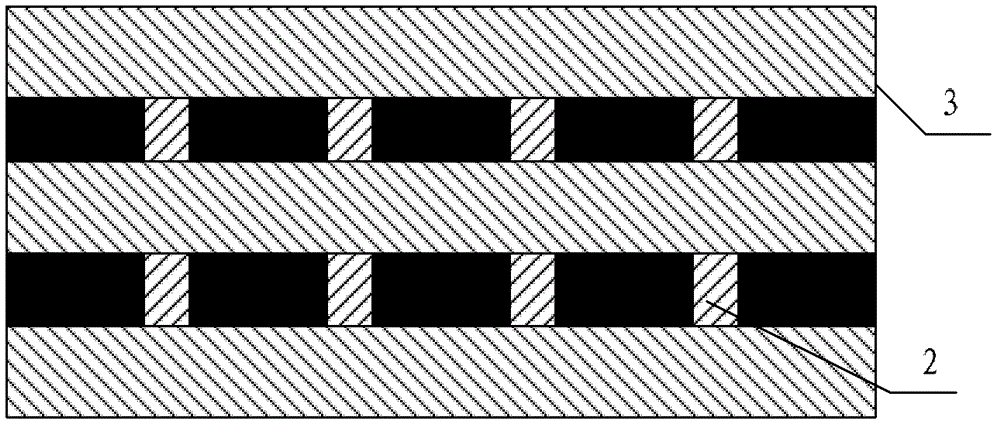
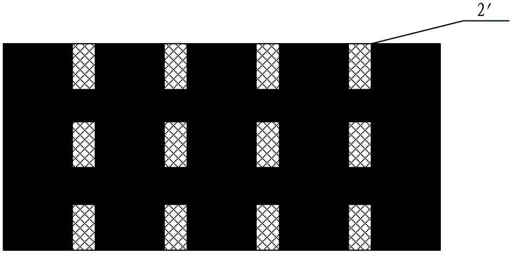
[0012] Such as Figure 2a As shown, on the semiconductor layer 21 to be etched (such as the polycrystalline gate layer), the first strip photoresist layer 22 is first formed by spin coating lithography or screen printing, and the first strip photoresist layer 22 is The resist layer 22 is subjected to freezing treatment ( Figure 2b ); Then form the second stripe photoresist layer 23 on the first stripe photoresist layer 22, the stripes of the second stripe photoresist layer 23 are orthogonal to the stripes of the first stripe photoresist layer 22, as Figure 2c As shown, and the thickness of the second stripe photoresist layer 23 is greater than the thickness of the first stripe photoresist layer 22, Figure 2d fo...


PUM


Abstract

The invention provides a photoetching method which includes the steps: forming rectangular photoresist on a semiconductor layer to be etched; and forming elliptical photoresist at one end or two ends of the rectangular photoresist to form similar bone-shaped patterned photoresist after the photoresist flows back. As corresponding photoresist positions prone to line edge shortening are compensated, rectangular edge shortening of the etched semiconductor layer caused by the LES (line edge shortening) effect is avoided, and the performance of a semiconductor device is improved.

Description

technical field [0001] The invention relates to the technical field of semiconductor device manufacturing, in particular to a photolithography method. Background technique [0002] Defects in the semiconductor manufacturing process are a major factor affecting the yield and performance of semiconductor devices. When manufacturing small-sized semiconductor devices, the process requirements for photolithography and etching processes are particularly strict. [0003] In the photolithography process, especially when making small-sized shapes, due to the optical diffraction effect and the etching itself cannot achieve 100% anisotropy, it will be difficult to achieve the desired shape after etching. For example, when forming rectangular thin strips by photolithography, due to the limitation of photolithography process, the photoresist with regular rectangular cubic structure cannot be formed; even if a regular rectangular cubic structure can be formed, in the subsequent etching p...

Claims


Application Information

Patent Timeline
Patent Type & Authority Patents(China)
IPC IPC(8): G03F7/00H01L21/308H01L21/3213
Inventor 王冬江孟晓莹周俊卿张海洋
Owner SEMICON MFG INT (SHANGHAI) CORP
Why Eureka
Try Eureka