InP-based mode division multiplexer/demultiplexer structure based on multimode interference coupler

A multi-mode interference and demultiplexer technology, applied in the field of InP-based waveguide devices, can solve problems such as incoupling

Active Publication Date: 2015-09-16
INST OF SEMICONDUCTORS - CHINESE ACAD OF SCI
View PDF3 Cites 18 Cited by
  • Summary
  • Abstract
  • Description
  • Claims
  • Application Information

AI Technical Summary

Problems solved by technology

However, this structure inevitably introduces additional loss, and because the output waveguide is inclined, it cannot be directly coupled with optical fibers and other devices

Method used


Image

  • InP-based mode division multiplexer/demultiplexer structure based on multimode interference coupler
  • InP-based mode division multiplexer/demultiplexer structure based on multimode interference coupler
  • InP-based mode division multiplexer/demultiplexer structure based on multimode interference coupler

Examples


Embodiment 1

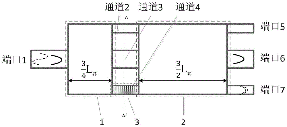
[0020] A mode-division multiplexer / demultiplexer structure based on a multimode interference coupler that realizes a π / 2 phase shift difference by increasing the effective refractive index of the phase shift region.

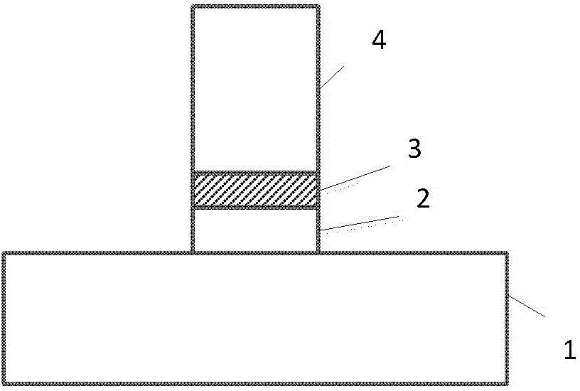
[0021] Such as figure 2 and image 3 As shown, the epitaxial material structure of the device is described as follows: First, an N-type InP buffer layer ② (thickness is 500nm) is epitaxially applied to an N-type InP substrate ①, and a 300nm-thick InGaAsP waveguide core layer ③ (with a bandgap wavelength of 1.3μm , and lattice-matched with InP), a 20nm-thick non-doped InP etch-stop layer, and a 100nm-thick InGaAsP waveguide core layer③ (its bandgap wavelength is 1.3μm, and it is lattice-matched with InP). Next, the 100nm-thick InGaAsP waveguide core layer in other regions except the phase shift region is etched away by photolithography and wet selective etching. Then second epitaxial 1.7μm thick non-doped InP waveguide capping layer ④.

[0022] figure 1 Dimen...

Embodiment 2

[0025] A mode-division multiplexer / demultiplexer structure based on a multimode interference coupler that achieves a π / 2 phase shift difference by reducing the effective refractive index of the phase shift region;

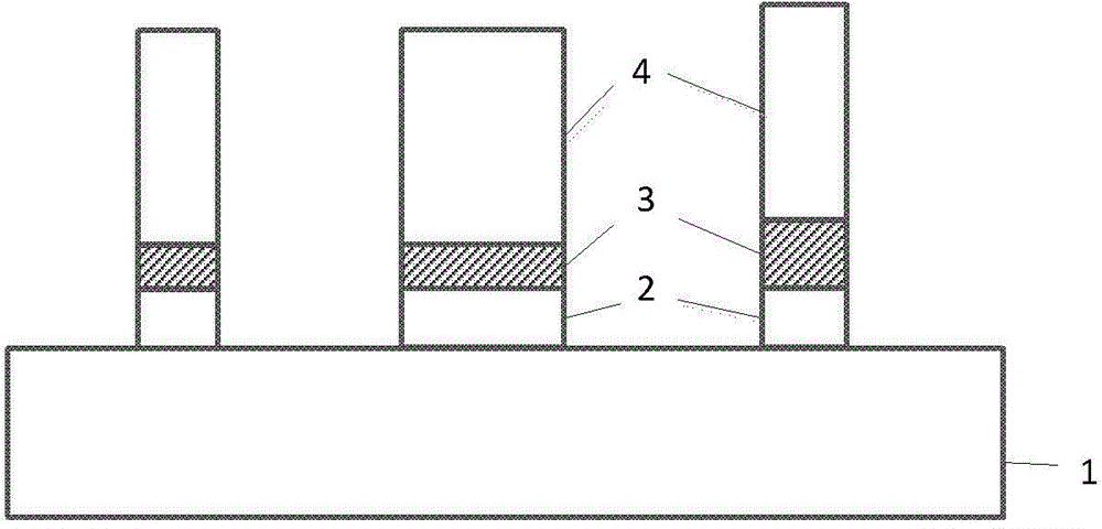
[0026] Such as figure 2 and Figure 4 As shown, the epitaxial material structure of the device is described as follows: First, an N-type InP buffer layer ② (thickness is 500nm) is epitaxially applied to an N-type InP substrate ①, and a 300nm-thick InGaAsP waveguide core layer ③ (with a bandgap wavelength of 1.3μm , and it is lattice-matched with InP), a 20nm-thick non-doped InP etch-stop layer, and a 100nm-thick InGaAsP waveguide core layer③ (its bandgap wavelength is 1.3μm, and it is lattice-matched with InP). Next, the 100nm-thick InGaAsP waveguide core layer in the phase shift region is etched away by photolithography and wet selective etching. Then second epitaxial 1.7μm thick non-doped InP waveguide capping layer ④.

[0027] figure 1Dimensions of the vari...


PUM


Abstract

The invention relates to an InP-based mode division multiplexer/demultiplexer structure based on a multimode interference coupler. The structure mainly comprises three parts which are a multimode interference coupler based mode conversion and separation structure, Pi/2 phase shift structure and a multimode interference coupler based 3dB coupler structure. In the Pi/2 phase shift structure, a transmission mode in a waveguide is enabled to be changed in phase shift through tuning the thickness of a waveguide core layer, and the phase shift change reaches Pi/2 when the length of the waveguide is a certain specific value. The mode multiplexer/demultiplexer structure has the advantages of compact structure, small device size, large channel bandwidth, low insertion loss and low channel crosstalk, and is simple in production process and high in production tolerance, thereby being very suitable for monolithic integration with devices such as a semiconductor laser, a modulator, an amplifier, a detector and the like, and being a key device for studying a mode division multiplexing technology based monolithic integration few-mode optical communication transmitting and receiving module.

Description

technical field [0001] The invention belongs to the technical field of few-mode optical communication, and specifically relates to a mode division multiplexing / demultiplexing device structure based on a multimode interference coupler phase-zone structure, which is a mode conversion and mode division multiplexing / demultiplexing device capable of realizing mode conversion and mode division multiplexing / demultiplexing. InP-based waveguide devices used. Background technique [0002] Due to the rapid development of the Internet in the optical fiber communication network, the sharp increase in the demand for system data rate and data capacity has put forward higher requirements for communication bandwidth and transmission rate, and expanding the transmission capacity of a single optical fiber has become the top priority. In order to improve the signal transmission capacity of the optical fiber communication network, technologies such as wavelength division multiplexing technology,...

Claims


Application Information

Patent Timeline
Patent Type & Authority Applications(China)
IPC IPC(8): G02B6/28
CPCG02B6/2813
Inventor 郭菲陆丹张瑞康王会涛王圩吉晨
Owner INST OF SEMICONDUCTORS - CHINESE ACAD OF SCI
Why Eureka
Try Eureka