Sub module of power semiconductor device

A technology of power semiconductors and sub-modules, which is applied in semiconductor devices, semiconductor/solid-state device parts, electric solid-state devices, etc., can solve problems such as easy wear of chips, unfavorable use, dislocation of chip plates, etc., and achieve normal electrical connection , Prevent wear, improve production qualification rate and service life

Active Publication Date: 2015-10-21
ZHUZHOU CRRC TIMES SEMICON CO LTD
View PDF4 Cites 10 Cited by
  • Summary
  • Abstract
  • Description
  • Claims
  • Application Information

AI Technical Summary

Problems solved by technology

[0003] In the prior art, the packaging structure of the sub-module of the power semiconductor device is relatively loose, so that the internal chip cannot be completely fixed, which easily leads to misalignment between the chip and the plates on both sides.
This dislocation makes it impossible for the chip to be electrically connected to the plate, which greatly affects the normal use of the sub-module of the power semiconductor device.
In addition, the chip is prone to dynamic friction with the polar plate when it is dislocated, so that the chip is extremely easy to wear, and then the sub-module of the power semiconductor device can no longer be used
This greatly affects the yield and service life of power semiconductor device sub-modules (especially insulated gate bipolar power semiconductor device sub-modules), which is very unfavorable for use

Method used


Image

  • Sub module of power semiconductor device
  • Sub module of power semiconductor device
  • Sub module of power semiconductor device

Examples


Embodiment Construction

[0024] The present invention will be further described below in conjunction with accompanying drawing.

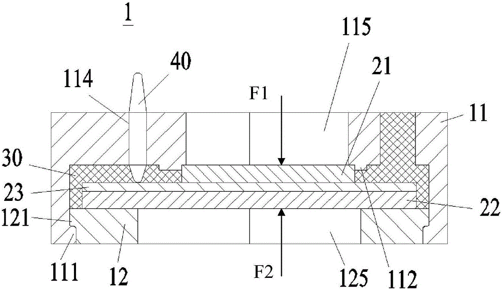
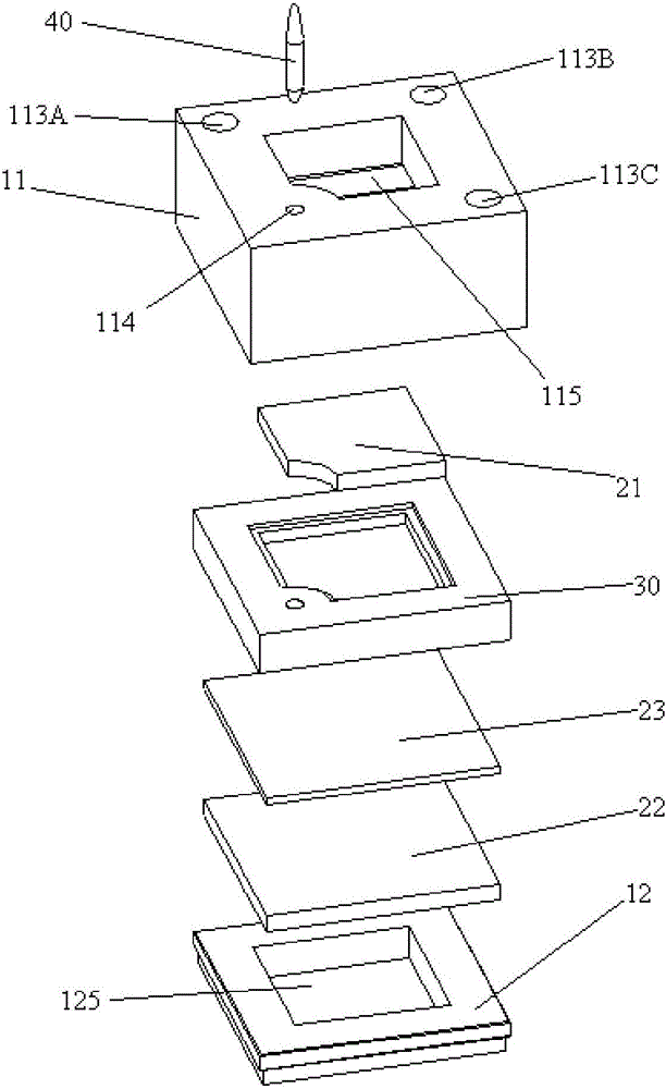
[0025] figure 1 The specific structure of the power semiconductor device sub-module 1 of the present invention is schematically shown. The power semiconductor device sub-module 1 includes a conductive component and a clamping component, and the conductive component is accommodated in the clamping component. The conductive component includes a first conductor 21 , a chip 23 and a second conductor 22 stacked in sequence, that is, the chip 23 is disposed between the first conductor 21 and the second conductor 22 . Both the first conductor and the second conductor can be pole plates or other conductive structures (for example, a molybdenum sheet with a certain thickness is usually used as the conductor). The first conductor 21 can be an emitter, and the second conductor 22 can be a collector. The clamping assembly can clamp the first conductor 21 and the second conductor 22,...


PUM


Abstract

The invention relates to a sub module of a power semiconductor device. The sub module includes a conducting assembly including a first conductor, a second conductor arranged opposite to the first conductor, a chip arranged between the first conductor and the second conductor in an overlapped manner; and a clamping assembly accommodating the conducting assembly. The clamping assembly can exert clamping forces on the first conductor and the second conductor along the overlapping direction. By using the sub module, dislocation of the chip between first conductor and the second conductor can be avoided.

Description

technical field [0001] The invention relates to the field of electronic integration, in particular to a sub-module of a power semiconductor device. Background technique [0002] The power semiconductor device sub-module is a commonly used transistor packaging structure. It is small in size and highly integrated, and is widely used in daily life and industrial processing. A power semiconductor device sub-module usually has a chip and a plate electrically connected to the chip. [0003] In the prior art, the packaging structure of the sub-module of the power semiconductor device is relatively loose, so that the internal chip cannot be completely fixed, which easily leads to misalignment between the chip and the plates on both sides. This dislocation makes it impossible for the chip to be electrically connected to the plate, which greatly affects the normal use of the sub-module of the power semiconductor device. In addition, the chip is prone to dynamic friction with the pol...

Claims


Application Information

Patent Timeline
IPC IPC(8): H01L23/32
Inventor 李继鲁窦泽春刘国友彭勇殿方杰常桂钦肖红秀
Owner ZHUZHOU CRRC TIMES SEMICON CO LTD
Why Eureka
Try Eureka