Sensor and manufacture method of the sensor

A manufacturing method and sensor technology, which are applied in semiconductor/solid-state device manufacturing, electric solid-state devices, semiconductor devices, etc., can solve the problems of inability to efficiently sense dynamic images and low carrier mobility of amorphous silicon materials.

Inactive Publication Date: 2015-11-18
AU OPTRONICS CORP
View PDF4 Cites 5 Cited by
  • Summary
  • Abstract
  • Description
  • Claims
  • Application Information

AI Technical Summary

Problems solved by technology

Generally speaking, the active element in the sensor can use amorphous silicon material as the channel layer, but the carrier mobility of amorphous silicon material is not high, so it cannot efficiently sense dynamic images

Method used


Image

  • Sensor and manufacture method of the sensor
  • Sensor and manufacture method of the sensor
  • Sensor and manufacture method of the sensor

Examples


Embodiment Construction

[0046] Below in conjunction with accompanying drawing, structural principle and working principle of the present invention are specifically described:

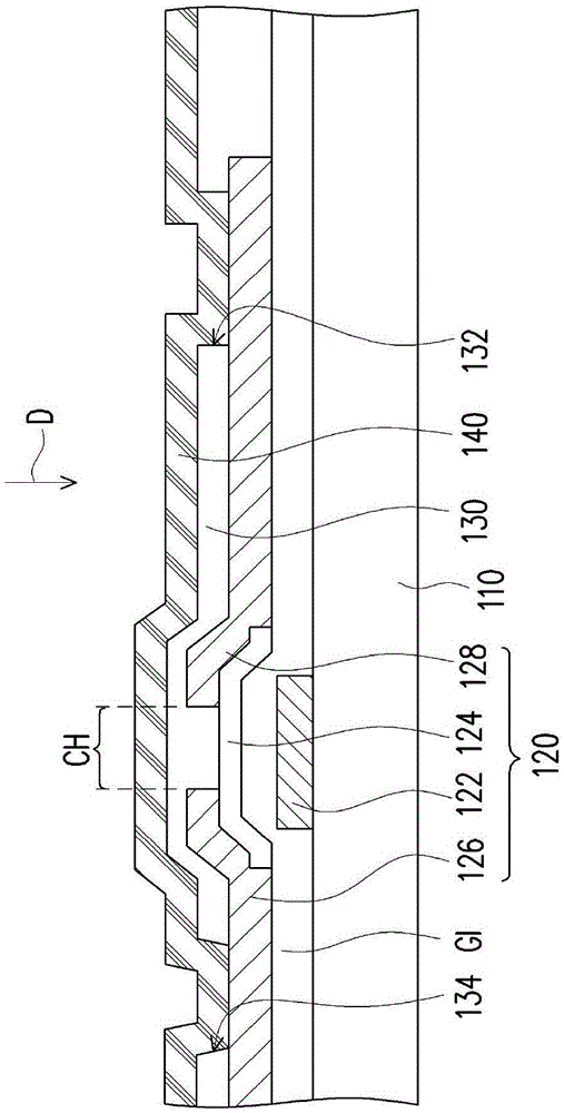
[0047] Figure 1A to Figure 1F It is the manufacturing method of the sensor of the first embodiment of the present invention. First, by Figure 1A It can be seen that the active device 120 is formed on the substrate 110 , where the active device 120 is, for example, a thin film transistor in this embodiment, and the active device 120 includes a gate 122 , a channel layer 124 , a source 126 and a drain 128 . The gate 122 is located between the channel layer 124 and the substrate 110 , and a gate insulating layer GI is disposed between the gate 122 and the channel layer 124 to avoid direct conduction between the two. Moreover, both the source electrode 126 and the drain electrode 128 are in contact with the channel layer 124 and are separated by a distance on the channel layer 124 to define the channel region CH. The above-men...


PUM


Abstract

A sensor and manufacture method of the sensor. The manufacture method comprises following steps: forming an active element on a substrate; forming a first insulation layer on the substrate for covering the ative element, wherein the first insulating layer has a first opening for locally exposing the active element; forming a blanket-covering type conductive layer made of conductive materials on the first insulation layer, wherein the blanket-covering type conductive layer is connected with the active element via the first opening; forming a photoelectric conversion material layer on the blanket-covering type conductive layer; forming a first photoresist pattern on the photoelectric conversion material layer, the first photoresist pattern serving as a mask; patterning and converting the photoelectric conversion material layer to a photoelectric conversion unit; patterning the blanket-covering type conductive layer to form a first electrode, wherein the first electrode is arranged in the first opening and enables the photoelectric unit to be electrically connected with the active element.

Description

technical field [0001] The invention relates to a sensor and a manufacturing method of the sensor, and in particular to a light sensor and a manufacturing method of this type of sensor. Background technique [0002] In recent years, with the development of optoelectronic technology, the application level of sensors has become wider and wider, and the sensing ability and sensing quality of sensors have also been improved. For sensors that can sense X-rays, due to their convenience and good image quality, they are very active in medical applications and developments. In order to achieve better sensing quality and even to sense moving images, transistors (or active elements) in the sensor are required to have higher performance. Generally speaking, the active element in the sensor can use amorphous silicon material as the channel layer, but the carrier mobility of the amorphous silicon material is not high, so it cannot efficiently sense dynamic images. Therefore, an oxide se...

Claims


Application Information

Patent Timeline
Patent Type & Authority Applications(China)
IPC IPC(8): H01L27/144H01L21/82
CPCH01L27/14612H01L27/14623H01L27/14663H01L27/14692H01L31/02164H01L31/022408H01L27/14685H01L31/02322H01L31/18
Inventor 郑造时陈盈宪徐文斌
Owner AU OPTRONICS CORP
Why Eureka
Try Eureka