Pixel structure, array substrate, display device and sub-pixel rendering method

A pixel array and pixel structure technology, applied in nonlinear optics, instruments, optics, etc., can solve the problems of increasing the number of data lines, reducing the pixel pitch, and increasing the difficulty of the process, so as to reduce the number, increase the sub-pixel pitch, The effect of saving data lines

Active Publication Date: 2015-11-25
XIAMEN TIANMA MICRO ELECTRONICS +1
View PDF5 Cites 5 Cited by
  • Summary
  • Abstract
  • Description
  • Claims
  • Application Information

AI Technical Summary

Problems solved by technology

[0006] 1. The number of sub-pixels increases by 1 / 3, the pixel pitch decreases, and the number of data lines increases, resulting in an increase in process difficulty;

Method used


Image

  • Pixel structure, array substrate, display device and sub-pixel rendering method
  • Pixel structure, array substrate, display device and sub-pixel rendering method
  • Pixel structure, array substrate, display device and sub-pixel rendering method

Examples


Embodiment Construction

[0028] The application will be further described in detail below in conjunction with the accompanying drawings and embodiments. It should be understood that the specific embodiments described here are only used to explain related inventions, rather than to limit the invention. It should also be noted that, for ease of description, only parts related to the invention are shown in the drawings.

[0029] It should be noted that, in the case of no conflict, the embodiments in the present application and the features in the embodiments can be combined with each other. The present application will be described in detail below with reference to the accompanying drawings and embodiments.

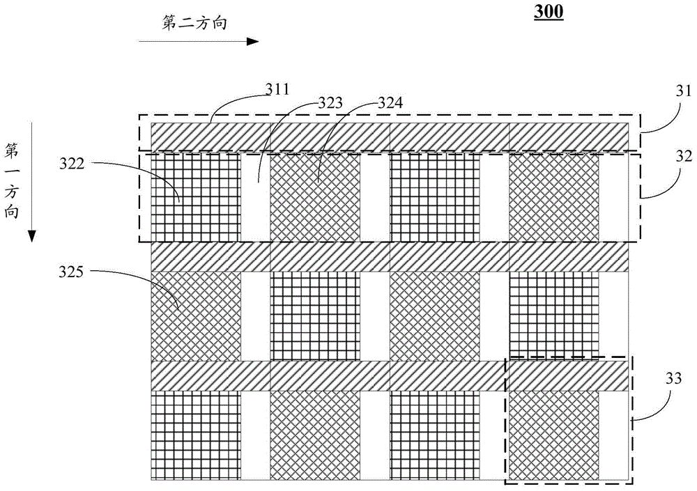
[0030] see image 3 Shown is a schematic structure diagram 300 of a pixel array in a pixel structure according to an embodiment of the present application.

[0031] The pixel structure of this embodiment includes such as image 3 The pixel array shown. Wherein, the pixel array includes a first ...


PUM


Abstract

The invention discloses a pixel structure, an array substrate, a display device and a sub-pixel rendering method. The pixel structure comprises a pixel array. The pixel array comprises first pixel sequences and second pixel sequences which are arranged at intervals in the first direction. The first pixel sequences comprise first sub-pixels arranged repeatedly in the second direction; the second pixel sequences comprise two different-color sub-pixels repeatedly arranged in an alternating mode in the second direction. The first direction is the horizontal or vertical direction. The second direction is perpendicular to the first direction. According to the scheme, the sub-pixels with the highest brightness in the pixel array can be distributed uniformly, so that it is ensured that the brightness of the whole pixel array is uniform, and the observation effects generated when the pixel array is observed from all view angles are uniform.

Description

technical field [0001] The present disclosure generally relates to display technology, specifically to sub-pixel rendering technology, and in particular to a pixel structure, an array substrate, a display device, and a sub-pixel rendering method. Background technique [0002] In current display products, with the continuous pursuit of high PPI (Pixel per Inch, pixels per inch), the transmittance will inevitably be compromised. In order to achieve high PPI and high transmittance at the same time, the W(White)R(Red)G(Green)B(Blue) design, which can greatly increase the transmittance, has gradually attracted attention. [0003] The size correspondence between traditional RGB pixels and traditional WRGB pixels is as follows: figure 1 shown. Each RGB pixel 110 has the same size as each WRGB pixel 120 . Specifically, the WRGB pixel 120 is formed by compressing the size of the three sub-pixels R, G, and B in one RGB pixel 110 and adding a W sub-pixel. [0004] Conventional WRGB...

Claims


Application Information

Patent Timeline
Patent Type & Authority Applications(China)
IPC IPC(8): G02F1/1333
CPCG02F1/1333
Inventor 雷萌周婷沈柏平张沼栋张少君
Owner XIAMEN TIANMA MICRO ELECTRONICS
Why Eureka
Try Eureka