A Method for Reducing the Edge Positioning Error of Optical Proximity Correction for Critical Dimensions

A technology of optical proximity correction and positioning error, which is applied to the photoplate process of optics and pattern surface, and the original for photomechanical processing, etc. It can solve problems such as EPE error, improve the process range, reduce manual debugging time, Effect of Small Edge Positioning Errors

Active Publication Date: 2019-09-27
SEMICON MFG INT (SHANGHAI) CORP
View PDF4 Cites 0 Cited by
  • Summary
  • Abstract
  • Description
  • Claims
  • Application Information

AI Technical Summary

Problems solved by technology

[0008] However, as chips become larger and more complex, there will be thousands of EPE errors
Therefore, manual debugging is unlikely to be an appropriate solution

Method used


Image

  • A Method for Reducing the Edge Positioning Error of Optical Proximity Correction for Critical Dimensions
  • A Method for Reducing the Edge Positioning Error of Optical Proximity Correction for Critical Dimensions
  • A Method for Reducing the Edge Positioning Error of Optical Proximity Correction for Critical Dimensions

Examples


Embodiment Construction

[0030] The embodiments of the present invention will now be described in detail with reference to the drawings. Reference will now be made in detail to the preferred embodiments of the present invention, examples of which are shown in the accompanying drawings. Wherever possible, the same signs will be used in all the drawings to indicate the same or similar parts. In addition, although the terms used in the present invention are selected from well-known and public terms, some of the terms mentioned in the specification of the present invention may be selected by the applicant according to his or her judgment. The detailed meanings are described herein. In the relevant part of the description. In addition, it is required to understand the present invention not only through the actual terms used, but also through the meaning contained in each term.

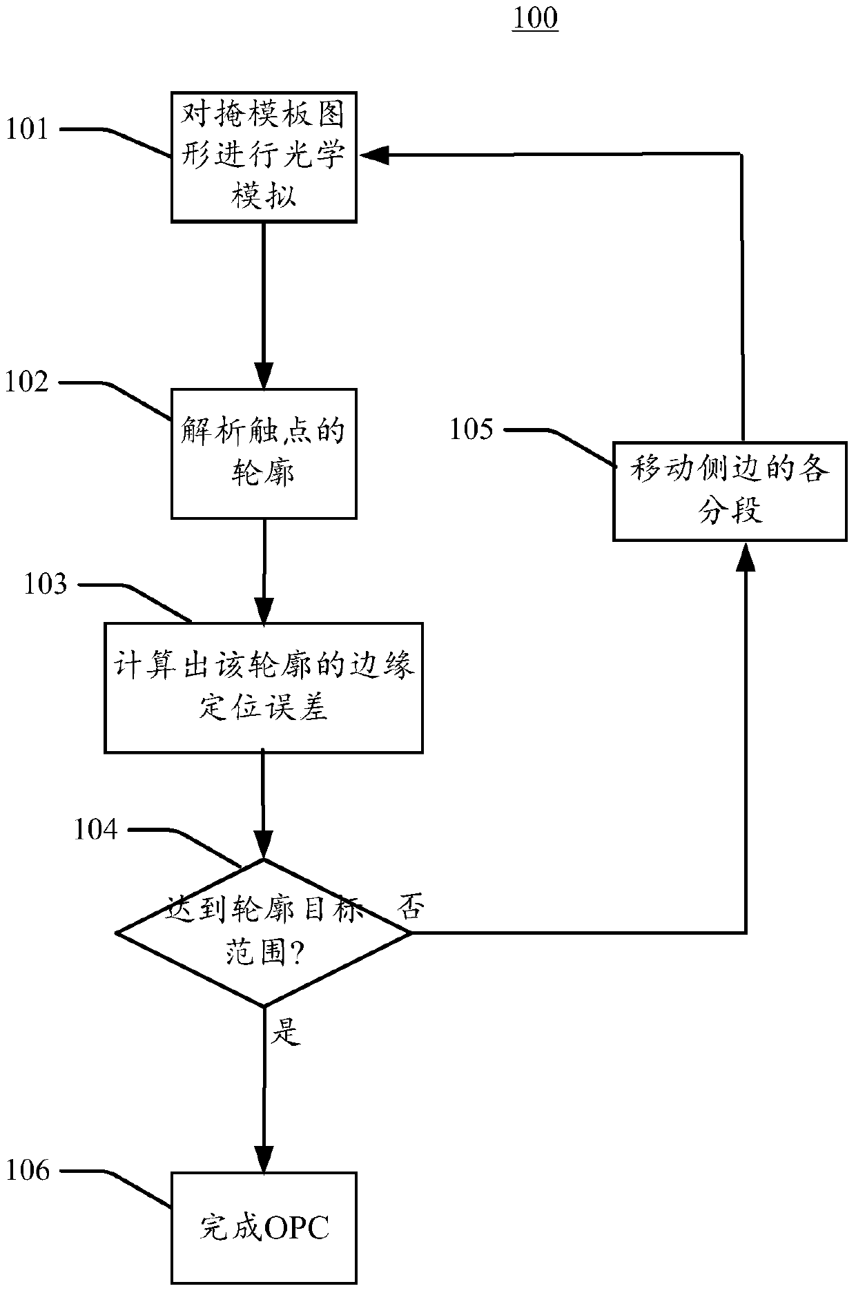
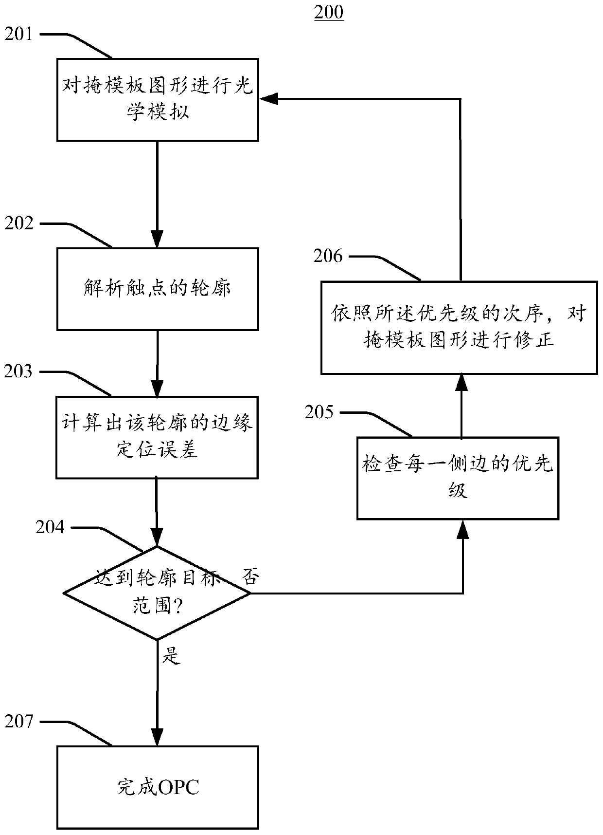
[0031] figure 2 A flowchart of the method according to the invention is shown. Such as figure 2 As shown, the method 200 for re...


PUM


Abstract

The invention provides a method for reducing edge placement error of critical dimension by optical proximity correction, comprising: a, performing optical simulation on mask plate graphics, wherein the mask plate graphics comprise through holes; b, analyzing the outlines of the through holes, wherein the outlines comprise multiple edges; c, calculating the edge placement error of the outlines; d, judging whether the edge placement error of the outlines reaches a preset outline target scope or not; e, if the edge placement error of the outlines exceeds the outline target scope, performing a step e1, examining the priority of each of the multiple edges of the outlines; e2, correcting the mask plate graphics according to the sequence of the priority; e3, replacing the mask plate graphics in the step a by the mask plate graphics corrected in the step e2, and re-executing the method for the mask plate graphics corrected in the step e2, and f, if the edge placement error of the outlines reaches the outline target scope, finishing the optical proximity correction on the mask plate graphics.

Description

Technical field [0001] The invention relates to the field of semiconductor manufacturing, and in particular to a method for reducing edge positioning errors of optical proximity correction. Background technique [0002] In the semiconductor manufacturing process, the photolithography process is at the center and is the most important process step in the production of integrated circuits. In order to overcome a series of optical proximity effects (Optical Proximity Effect, OPE) due to the reduction of critical dimensions (CD), the industry has adopted many Resolution Enhancement Technology (RET), including optical proximity correction ( Optical Proximity Correction, OPC), Phase Shifting Mask (PSM) and other technologies. [0003] Optical proximity correction is mainly to compare the simulated graphics to be exposed with the target graphics, establish a correction mode for the graphics to be exposed, and then use the simulator to perform a series of complex correction calculations b...

Claims


Application Information

Patent Timeline
Patent Type & Authority Patents(China)
IPC IPC(8): G03F1/36
Inventor 张婉娟
Owner SEMICON MFG INT (SHANGHAI) CORP
Why Eureka
Try Eureka