Pixel structure

A pixel structure and pixel technology, applied in nonlinear optics, instruments, optics, etc., can solve the problem of color shift that needs to be strengthened, and achieve the effect of improving the color shift problem

Active Publication Date: 2015-12-02
AU OPTRONICS CORP
View PDF5 Cites 15 Cited by
  • Summary
  • Abstract
  • Description
  • Claims
  • Application Information

AI Technical Summary

Problems solved by technology

However, such improvements are more effective in improving color saturation, but the effect on improving color cast still needs to be strengthened

Method used


Image

  • Pixel structure
  • Pixel structure
  • Pixel structure

Examples


no. 1 example

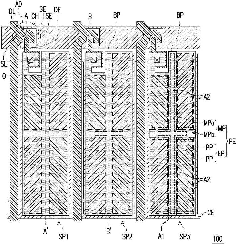
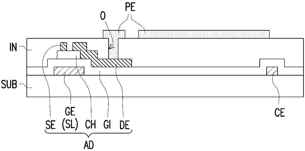
[0055] Figure 1A is a schematic top view of a pixel structure according to the first embodiment of the present invention, wherein Figure 1A Partial film layers are omitted. Figure 1B and Figure 1C are along Figure 1A Schematic cross-sectional view of the middle line A-A', B-B'. Please refer to Figure 1A to Figure 1C , the pixel structure 100 of this embodiment includes a plurality of sub-pixels arranged in an array, such as a first sub-pixel SP1, a second sub-pixel SP2 and a third sub-pixel SP3. The sub-pixels are arranged, for example, on the substrate SUB. In addition, a plurality of scanning lines SL may be further arranged on the substrate SUB ( Figure 1A Only one scan line SL) and multiple data lines DL are schematically shown. The scan lines SL and the data lines DL intersect each other to define the area where each sub-pixel is located. In addition, each sub-pixel is suitable to be driven by one of the scan lines SL and one of the data lines DL.

[0056] Fur...

no. 2 example

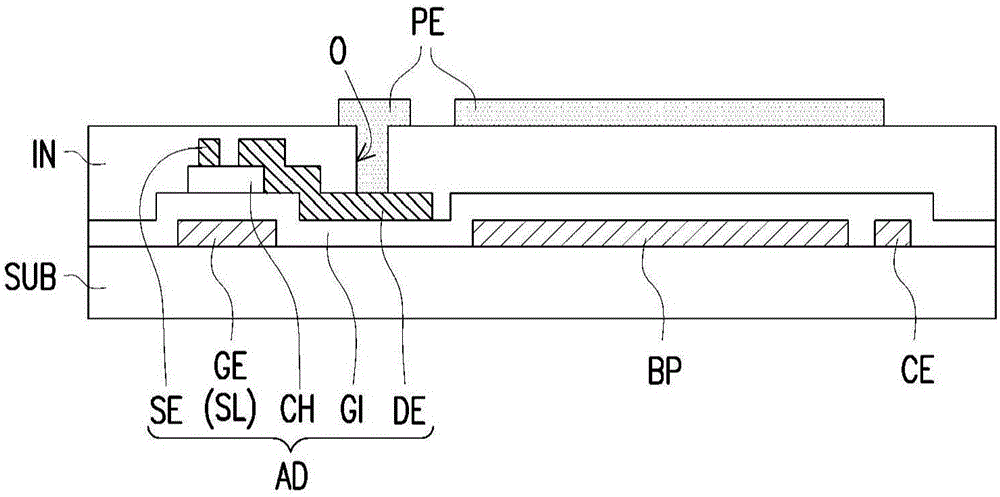
[0075] Figure 2 to Figure 8 is a schematic top view of various pixel structures according to the second embodiment of the present invention, wherein Figure 2 to Figure 8 Partial film layers are omitted. The design concept of the pixel structure 200 in this embodiment is similar to that of the pixel structure 100 in the first embodiment, the main difference is that the first sub-pixel SP1 in the pixel structure 200 of this embodiment has a light-shielding area corresponding to the staggered area pattern BP, and the first sub-pixel SP1 in the pixel structure 100 of the first embodiment does not have the light-shielding pattern BP corresponding to the misalignment area A1. Figure 1 with Figure 2 to Figure 8 The same or similar elements are denoted by the same or similar reference numerals.

[0076] Please refer to Figure 2 to Figure 8 The pixel structures 200A-200G in this embodiment include a plurality of sub-pixels arranged in an array (such as a first sub-pixel SP1, a ...


PUM


Abstract

The invention relates to a pixel structure, which comprises a plurality of sub-pixels arranged in an array. Each of the sub-pixels comprises an active component and a pixel electrode electrically connected with the active component. Each of the pixel electrodes separately defines misorientation regions and a plurality of display region separated by the misorientation regions, wherein only a part of the sub-pixels further comprises shading patterns corresponding to the misorientation regions.

Description

technical field [0001] The present invention relates to a pixel structure, and in particular to a pixel structure that helps to improve the problem of color shift in side view. Background technique [0002] Liquid crystal displays with excellent space utilization efficiency, low power consumption, and no radiation have gradually become the mainstream of the market. In order to improve the display quality of liquid crystal displays, various liquid crystal displays with wide viewing angles have been developed on the market, such as in-plane switching (IPS) liquid crystal displays, fringe field switching (fringe field switching) liquid crystal displays and Multi-domain vertical alignment (multi-domain vertical alignment, MVA) liquid crystal display, etc. [0003] Although the multi-domain vertical alignment liquid crystal display has the effect of wide viewing angle, its light transmittance will vary with the viewing angle. That is to say, when the user looks at the display s...

Claims


Application Information

Patent Timeline
Patent Type & Authority Applications(China)
IPC IPC(8): G02F1/1335G02F1/1343
CPCG02F1/133512G02F1/134309G02F1/133707G02F1/134336G02F1/136209
Inventor 田堃正廖乾煌李书恩
Owner AU OPTRONICS CORP
Why Eureka
Try Eureka