Thin film transistor, fabrication method thereof, array substrate and display panel

A technology for thin film transistors and array substrates, applied in the field of semiconductor bodies, can solve the problems of performance deterioration of thin film transistors, no switching performance of oxide thin film transistors, destruction of metal oxide active layers, etc.

Inactive Publication Date: 2015-12-09
BOE TECH GRP CO LTD
View PDF4 Cites 10 Cited by
  • Summary
  • Abstract
  • Description
  • Claims
  • Application Information

AI Technical Summary

Problems solved by technology

[0004] At present, in the process of preparing an oxide thin film transistor, the source electrode layer and the drain electrode layer are formed after the metal oxide active layer is formed, but the etching of the source and drain electrodes will cause certain damage to the metal oxide active layer. Although the degree of damage can be improved by adjusting the etching solution, it cannot be avoided, which will cause the performance of the thin film transistor to deteriorate, and even cause the oxide thin film transistor to have no switching performance.

Method used


Image

  • Thin film transistor, fabrication method thereof, array substrate and display panel
  • Thin film transistor, fabrication method thereof, array substrate and display panel
  • Thin film transistor, fabrication method thereof, array substrate and display panel

Examples


Embodiment 1

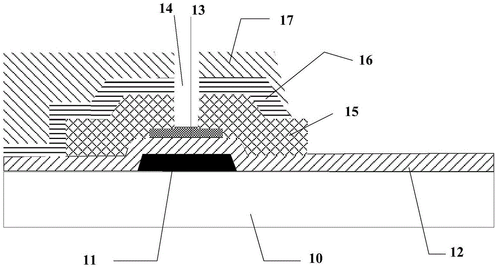
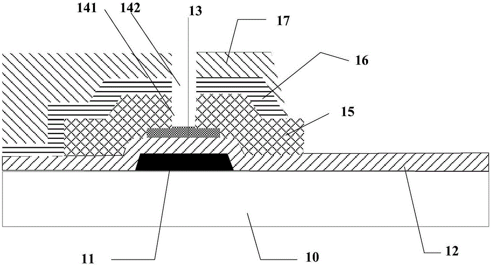
[0037] A thin film transistor provided by Embodiment 1 of the present invention, such as Figure 1a As shown, it includes: a base substrate 10, a gate electrode 11, a gate insulating layer 12, an active layer 13, and a source-drain electrode 15 located on the base substrate 10 in sequence; it also includes:

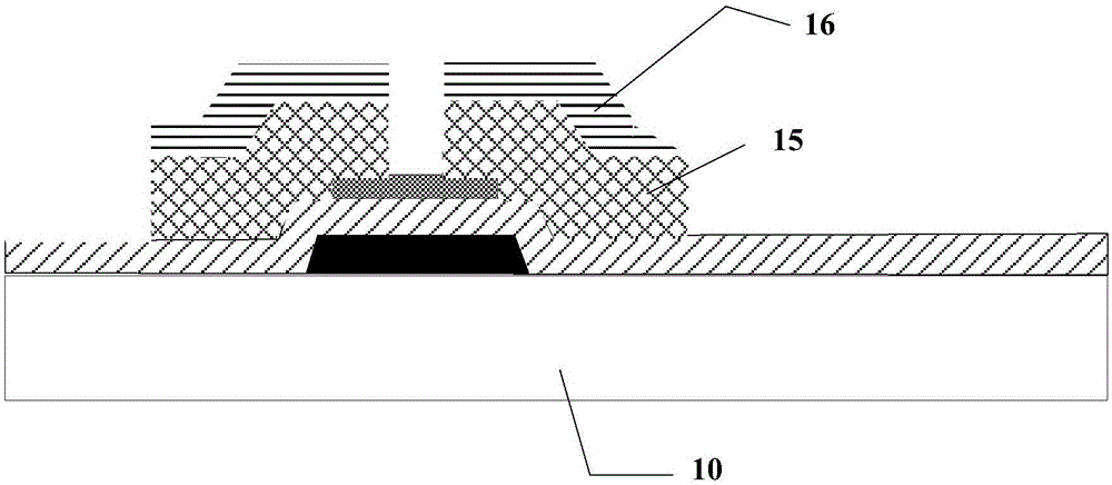
[0038] An oxidation protection layer 16 disposed on the source-drain electrodes 15 .

[0039] Through the opening 14 of the oxidation protection layer 16 , the opening 14 corresponds to the active layer region between the source and drain electrodes 15 .

[0040] In the thin film transistor provided by the embodiment of the present invention, an oxidation protection layer is provided on the source and drain electrodes, which avoids the problem that the source and drain electrodes are oxidized during the formation process and affects the performance of the thin film transistor. It is precisely because the oxide protection layer is provided on the source and drain electrode...

Embodiment 2

[0073] Based on the same inventive concept, Embodiment 2 of the present invention also provides a method for manufacturing a thin film transistor, which includes: sequentially forming the active layer of the thin film transistor, forming the thin film of the source and drain electrode layers of the thin film transistor, and forming the oxidation protection layer of the thin film transistor. layer film, forming the first opening of the channel region of the active layer corresponding to the source and drain electrode layer film, and forming the second opening of the channel region of the active layer corresponding to the oxidation protective layer film, wherein the first opening and the second The openings are formed by one patterning process. The specific process is as image 3 As shown, the following are detailed descriptions:

[0074] 301. Form a pattern of a gate electrode on a base substrate.

[0075] The base substrate can be a transparent glass substrate or quartz.

...

Embodiment approach

[0095] The first implementation mode: the active layer, the source and drain electrodes of the thin film transistor and the oxidation protection layer of the thin film transistor can be formed through one patterning process.

[0096] Specifically, such as Figure 4g As shown, the active layer 231 , the source and drain electrodes 241 of the thin film transistor and the oxidation protection layer 251 of the thin film transistor are formed by one patterning process.

[0097] Preferably, the active layer, the source and drain electrodes of the thin film transistor and the oxidation protection layer of the thin film transistor can be formed through a halftone mask or a gray scale mask.

[0098] The second implementation manner: before the step of forming the first opening, the method further includes: forming an active layer and a source-drain electrode layer film without the first opening through a patterning process. The resin layer of the thin film transistor, the oxidation pr...


PUM


Abstract

The invention discloses a thin film transistor, a fabrication method thereof, an array substrate and a display panel. The thin film transistor comprises a substrate, an active layer, a source electrode and a drain electrode and also comprises an oxide protective layer and an opening, wherein the active layer is arranged on the substrate, the source electrode and the drain electrode are arranged on the active layer, the oxide protective layer is arranged on the source electrode and the drain electrode, and the opening passes through the oxide protective layer and is in corresponding to an active layer region between the source electrode and the drain electrode. By the thin film transistor, the fabrication method thereof, the array substrate and the display panel, the drain electrode can be prevented from being oxidized, and thus, the performance of the thin film transistor is enhanced.

Description

technical field [0001] The invention relates to the field of semiconductor technology, in particular to a thin film transistor, a preparation method thereof, an array substrate and a display panel. Background technique [0002] With the development of the flat panel display industry, the requirements for the display panel are getting higher and higher, and the mobility of the thin film transistor in the panel is also higher. At present, the existing thin film transistor (ThinFilmTransistor, TFT) is generally an amorphous silicon thin film transistor, and the active layer of the amorphous silicon thin film transistor is amorphous silicon material, and the carrier mobility of the amorphous silicon thin film transistor Low, its electron mobility is 0.1-1cm 2 V -1 the s -1 , can not adapt to the current development of the display industry. Therefore, a low temperature polysilicon (LTPS, Low Temperature PolySilicon) thin film transistor and an oxide (Oxide) thin film transist...

Claims


Application Information

Patent Timeline
Patent Type & Authority Applications(China)
IPC IPC(8): H01L29/786H01L21/336H01L27/12
CPCH01L27/1214H01L29/66742H01L29/7869H01L27/1225H01L27/1248H01L29/41733H01L23/53295H10K59/121H10K59/124G02F1/1368H01L27/1288H01L29/66969
Inventor 刘翔
Owner BOE TECH GRP CO LTD
Why Eureka
Try Eureka