AI technical title is built by Patsnap AI team. It summarizes the technical point description of the patent document.
A technology for array substrates and devices, which is applied in the field of OLED devices and array substrates, and can solve problems such as uneven luminescence
Inactive Publication Date: 2015-12-09
TCL CHINA STAR OPTOELECTRONICS TECH CO LTD
View PDF4 Cites 19 Cited by
Summary
Abstract
Description
Claims
Application Information
AI Technical Summary
This helps you quickly interpret patents by identifying the three key elements:
Problems solved by technology
Method used
Benefits of technology
Problems solved by technology
[0005] The purpose of the present invention is to provide an OLED device and a display panel to solve the technical problem of uneven light emission of existing OLED devices
Method used
Image
Click on the blue label to locate the original text in one second.
Reading with bidirectional positioning of images and text.
Examples
Embodiment 1
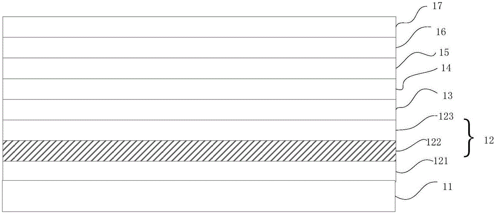
[0055] refer to figure 1 , the present embodiment provides an OLED device, comprising:
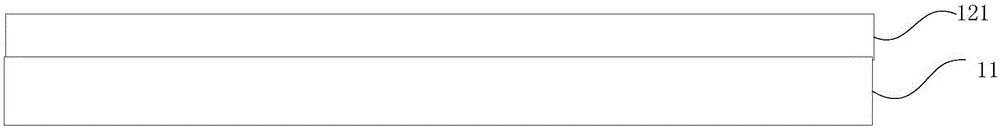
[0056] Substrate substrate 11, preferably a glass substrate;
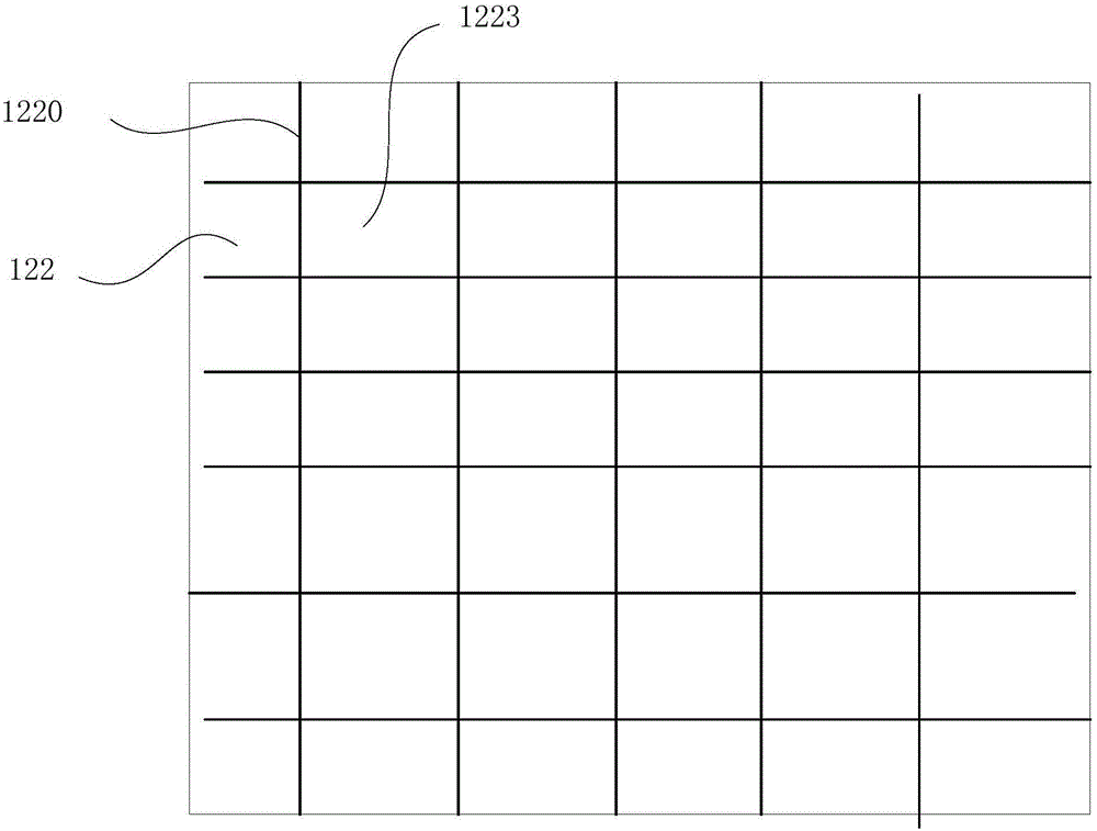
[0057] The transparent anode 12 is arranged on the substrate 11, and is used to output holes (or called carriers) under voltage driving; for example, when the OLED device is in operation, the transparent anode 12 is connected to the positive pole of the driving voltage, and the transparent cathode 17 is connected to the positive pole of the driving voltage. The negative pole of the driving voltage;
[0058] A hole injection layer 13, disposed on the transparent anode layer 12, for receiving holes output by the transparent anode;
[0059] The hole transport layer 14 is arranged on the hole injection layer 13, and is used to transport the holes in the hole injection layer to the organic light-emitting layer 15; the hole transport layer 14 in this embodiment can reduce the transparent anode 12 The interface barrier between the ...
Embodiment 2
[0088] This embodiment provides an OLED array substrate, comprising:
[0089] Substrate substrate;
[0090] OLED devices, arranged on the substrate substrate;
[0091] A thin film transistor, arranged on the substrate, is used to control the corresponding OLED device to emit light;
[0092] OLED device, reference figure 1 ,include:
[0093] The transparent anode 12 is arranged on the substrate 11 and is used to output holes under voltage driving; for example, when the OLED device is in operation, the transparent anode 12 is connected to the positive pole of the driving voltage, and the transparent cathode 17 is connected to the negative pole of the driving voltage;
[0094] A hole injection layer 13, disposed on the transparent anode layer 12, for receiving holes output by the transparent anode;
[0095] The hole transport layer 14 is arranged on the hole injection layer 13, and is used to transport the holes in the hole injection layer to the organic light-emitting layer ...
PUM
Abstract
The invention provides an OLED device and an array substrate. The embodiments of the invention provide an OLED device which is configured such as that: two transparent anode layers are arranged, and a metal layer is arranged between the two transparent anode layers so as to reduce resistance of the transparent anodes in a horizontal direction. The OLED device increases horizontal conductivity of the transparent anodes, addresses the problem of uneven light emission caused by large horizontal resistance of the transparent anodes for OLED devices, and increases quality of image displaying.
Description
【Technical field】 [0001] The invention relates to the field of display technology, in particular to an OLED (organic light emitting diode) device and an array substrate. 【Background technique】 [0002] At present, in the working process of a large-area OLED (Organic Light Emitting Diode) display panel, uneven light emission often occurs. There are many reasons for this phenomenon. The main reasons are uneven distribution of vertical resistance and excessive horizontal resistance. Among them, the vertical resistance is mainly determined by the energy level structure of the device, the carrier mobility and the thickness of each film layer; the horizontal resistance is determined by the conductivity of the transparent electrode. [0003] At present, it is difficult to make a transparent electrode with low level resistance, so the horizontal resistance (that is, the resistance in the horizontal direction) of the transparent anode is relatively high at present. When the OLED is ...
Claims
Application Information
Patent Timeline
Application Date:The date an application was filed.
Publication Date:The date a patent or application was officially published.
First Publication Date:The earliest publication date of a patent with the same application number.
Issue Date:Publication date of the patent grant document.
PCT Entry Date:The Entry date of PCT National Phase.
Estimated Expiry Date:The statutory expiry date of a patent right according to the Patent Law, and it is the longest term of protection that the patent right can achieve without the termination of the patent right due to other reasons(Term extension factor has been taken into account ).
Invalid Date:Actual expiry date is based on effective date or publication date of legal transaction data of invalid patent.

