Electroluminescent device, manufacturing method of electroluminescent device and display device

一种电致发光器件、发光层的技术,应用在电致发光光源、电光源、电气元件等方向,能够解决易受水分的影响、发光亮度低、发光效率低等问题,达到解决发光不均匀、提高发光亮度、提高发光效率的效果

Inactive Publication Date: 2014-07-23
BOE TECH GRP CO LTD +1
View PDF5 Cites 1 Cited by
  • Summary
  • Abstract
  • Description
  • Claims
  • Application Information

AI Technical Summary

Problems solved by technology

[0002] Liquid Crystal Display (LCD for short) is widely used as a flat display device. Because it does not use self-luminous components, it needs additional light-emitting components, such as a backlight (Backlight). Difficult to simplify
Active Matrix Organic Light Emitting Diode (OLED) is a new type of display technology developed in recent years. Because it uses self-luminous components, it overcomes the above problems of LCD and does not require a backlight. And has a relatively simple structure, but because there are few organic materials that can be used in OLEDs, and these organic materials are easily affected by moisture, so it has strict requirements on the vacuum deposition process. In order to overcome the above limitations, some high-tech methods have been used Molecular materials, and other methods have been found, such as inkjet method, laser-induced thermal imaging method, etc. However, the methods and components that meet the above requirements have not been practically applied. Therefore, compared with organic light-emitting diodes, inorganic semiconductors Luminescence still has a good application prospect
[0003] At present, for inorganic light-emitting diodes, whether it is gallium nitride (GaN) that emits blue-green light or aluminum gallium indium phosphide (AlGaInP) that emits red and yellow light, the luminous efficiency of the light-emitting layer inside the light-emitting diode element is very high. Due to the problems of refraction and light absorption of each layer of material inside the diode, the actual light output efficiency outside the LED element is not high, and most of the light cannot be taken out. Therefore, the luminous efficiency of the existing inorganic light-emitting diodes is low. low brightness

Method used


Image

  • Electroluminescent device, manufacturing method of electroluminescent device and display device
  • Electroluminescent device, manufacturing method of electroluminescent device and display device
  • Electroluminescent device, manufacturing method of electroluminescent device and display device

Examples


Embodiment 1

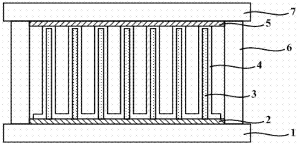
[0088] Such as Figure 5a As shown, Figure 5a In order to fabricate the structure diagram of the electroluminescent device with the alignment layer, the alignment layer 10 is fabricated on the back plate 1 where the driving circuit and the first electrode 2 have been prepared. The alignment layer 10 is made of the same material as the nanowire, and has a thickness of about 50%. ~2000 Angstroms. In this embodiment, the orientation layer 10 is a P-type film, and the first electrode 2 is a transparent conductive layer, such as indium tin oxide (ITO), indium zinc oxide (IZO), indium gallium zinc oxide (IGZO) or For other transparent conductive semiconductor films, the backplane 1 needs to be etched in advance for supporting insulating materials, such as SiO 2 ;

[0089] Such as Figure 5b As shown, Figure 5b In order to complete the structure diagram of the electroluminescent device with nanowires, in a vacuum environment, the back plate with the alignment layer 10 is heated to a ce...

Embodiment 2

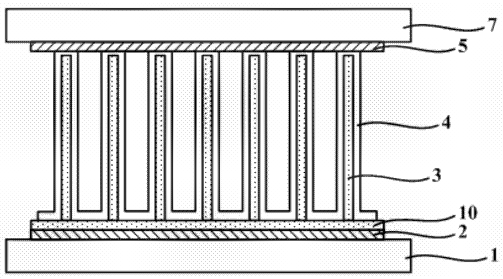
[0095] Please continue to refer Figure 5a As shown, an orientation layer 10 is fabricated on the back plate 1 on which the drive circuit and the first electrode 2 have been prepared. The material of the orientation layer 10 is the same as that of the nanowires. In this embodiment, the orientation layer 10 is a P-type film. The electrode 2 is a transparent conductive layer, and the back plate 1 needs to be etched in advance for supporting insulating materials, such as SiO 2 , The thickness is about 50~2000 angstroms;

[0096] Please continue to refer Figure 5b As shown, in a vacuum environment, the backplane with the orientation layer 10 is heated to a certain temperature range, such as 150°C to 600°C, and the single crystal P-type nanowires are grown on the orientation layer 10 by the VS (Vapor Solid) method 3. The catalyst is Ga, and the source gas will self-nucleate into GaAs nanowires with a single crystal orientation and uniform morphology during the deposition process. Acco...

Embodiment 3

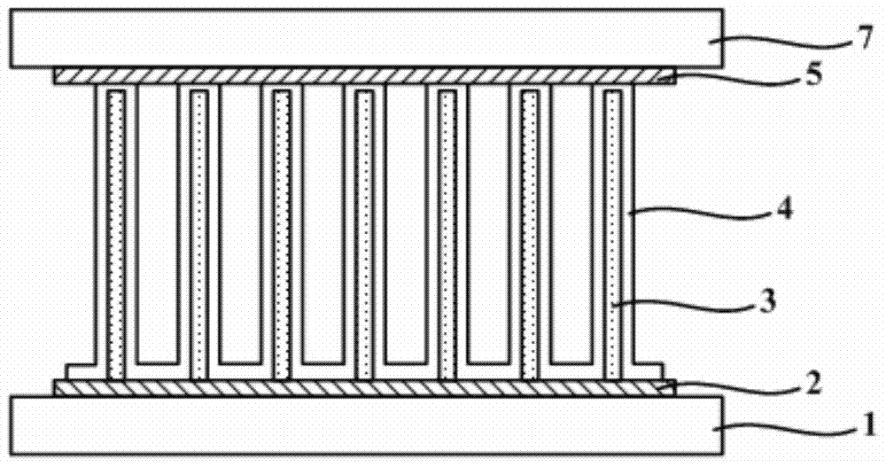
[0102] Please continue to refer Figure 5a As shown, the alignment layer 10 is made after the drive circuit and the first electrode 2 have been prepared. The alignment layer 10 is made of the same material as the nanowire, and has a thickness of about 50-2000 angstroms. The first electrode 2 is a reflective metal cathode, such as aluminum. (Al), molybdenum tungsten alloy (MoW), molybdenum neodymium alloy (MoNd), aluminum neodymium alloy (AlNd) or other metals or alloys that can be used as cathode materials. The back plate 1 needs to be etched in advance for supporting insulation Material, such as SiO 2 ;

[0103] Please continue to refer Figure 5b As shown, in a vacuum environment, the backplane with the orientation layer 10 is heated to a certain temperature range, such as 150°C to 600°C, and the single crystal N-type nanowire 3 is grown on the orientation layer 10 by the VLS method. The catalyst is Au, the source gas self-nucleates during the deposition process into nanowires ...


PUM

PropertyMeasurementUnit
lengthaaaaaaaaaa
diameteraaaaaaaaaa
sizeaaaaaaaaaa

Abstract

The invention relates to the technical field of display and discloses an electroluminescent device, a manufacturing method of the electroluminescent device and a display device. The electroluminescent device comprises a first electrode, a second electrode opposite to the first electrode, and a luminescent layer located between the first electrode and the second electrode. The luminescent layer comprises nanowires and a coating layer, wherein the nanowires are located on the first electrode and distributed in an array mode and is in the first conduction type, the nanometers are coated with the coating layer which is in the second conduction type, and the coating layer is electrically connected with the second electrode. According to the technical scheme, due to the fact that the diameter of the nanowires is only tens of nanometers and is far smaller than the luminescent wavelength, light can directly penetrate through the nanowires to be emitted out, no refraction problem exists basically, light emitted by most light emitting diodes can be taken out, then the luminescent efficiency of the electroluminescent device is greatly improved, and luminance is improved.

Description

Technical field [0001] The invention relates to the field of display technology, in particular to an electroluminescent device, a preparation method thereof, and a display device. Background technique [0002] Liquid Crystal Display (LCD for short) is widely used as a flat display device. Because it does not use self-luminous elements, additional light-emitting elements, such as backlights, are required. Therefore, the liquid crystal display has a relatively large thickness and a relatively large structure. Difficult to simplify. Active Matrix Organic Light Emitting Diode (OLED) is a new type of display technology developed in recent years. Because it uses self-luminous elements, it overcomes the above-mentioned problems of LCD and does not require a backlight. It has a relatively simple structure, but because there are fewer organic materials that can be used in OLEDs and these organic materials are susceptible to moisture, they have strict requirements on the vacuum deposition...

Claims


Application Information

Patent Timeline
Patent Type & Authority Applications(China)
IPC IPC(8): H01L33/48H01L33/58H01L33/56
CPCH05B33/14B82Y20/00H05B33/10H05B33/22Y10S977/762Y10S977/95H01L33/38H01L33/005H01L33/06
Inventor 王劭颛
Owner BOE TECH GRP CO LTD
Why Eureka
Try Eureka