Light guide and high uniformity and high brightness light source module

A technology of light guide components and light source modules, which is applied in the direction of optical components, semiconductor devices of light-emitting components, light sources, etc., which can solve the problems of poor light utilization, inability to effectively use LEDs, uneven light output, etc., and achieve the goal of overcoming light utilization. bad effect

Inactive Publication Date: 2014-10-15
ATEN INT CO
View PDF5 Cites 2 Cited by
  • Summary
  • Abstract
  • Description
  • Claims
  • Application Information

AI Technical Summary

Problems solved by technology

However, this design will not be able to effectively utilize the light emitted from the side of the LED, making the light utilization rate poor, and the asymmetric structure also causes uneven light output

Method used


Image

  • Light guide and high uniformity and high brightness light source module
  • Light guide and high uniformity and high brightness light source module
  • Light guide and high uniformity and high brightness light source module

Examples


Embodiment Construction

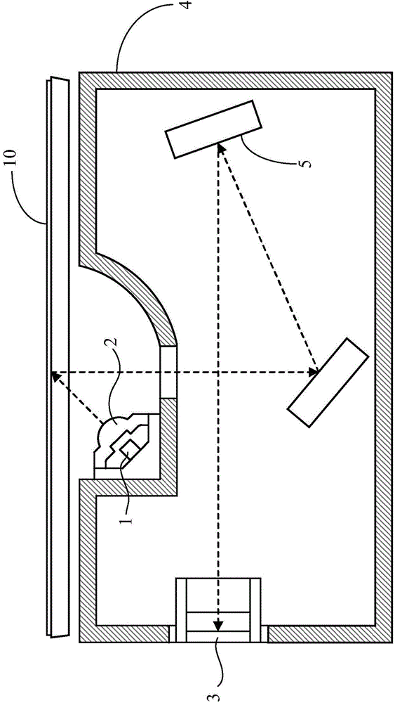
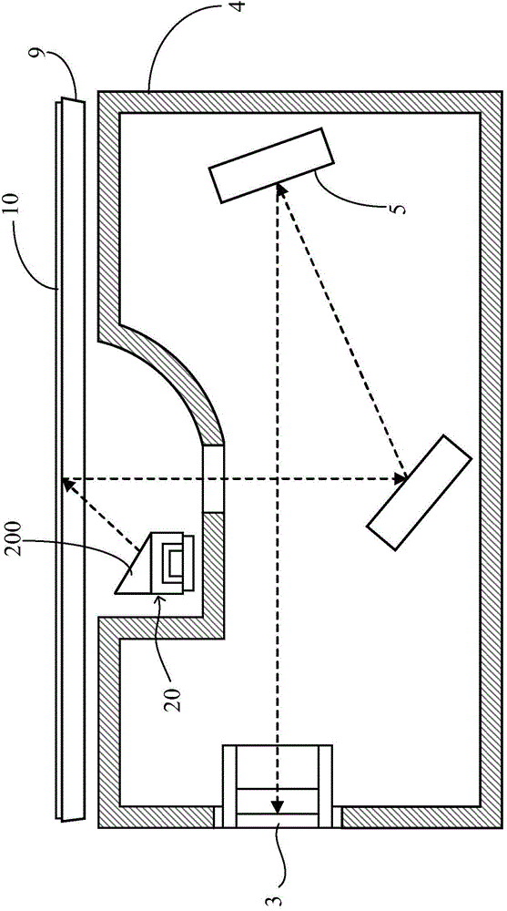
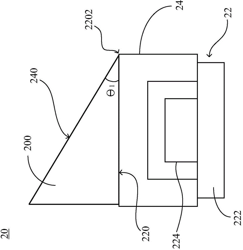
[0024] The first preferred embodiment of the light guide element of the present invention will be described in detail below with reference to the accompanying drawings, wherein the same reference numerals in different drawings represent the same or similar components. Please refer to figure 2 , figure 2 A schematic cross-sectional view of a contact image sensor according to a first preferred embodiment of the present invention is shown, wherein the light source module of this preferred embodiment is represented by symbol 20, and the light guide element of this preferred embodiment is represented by symbol 200 .

[0025] The contact image sensor includes a light source module 20 with high uniformity and high brightness, a photosensitive unit array 3 , a strip-shaped square box 4 , multiple reflectors 5 , and a light-transmitting plate 9 . When scanning the document 10, the light source module 20 irradiates light onto the document 10, and after the incident light is reflecte...


PUM


Abstract

The invention discloses a light guide for a contact image sensor. The light guide is utilized to import the light emitted from a LED light bar. The light guide includes a strip-type incident plane and an exit plane. An acute angle is interposed between the strip-type incident plane and the LED light bar at a short side of the LED light bar. The strip-type incident plane has a plurality of micro structures which are used to diffuse the light toward a uniform direction, thereby increasing light utilization efficiency.

Description

[0001] The patent application for the present invention is a divisional application. The application number of the original case is: 201110151364.6; the application date is: June 8, 2011; the title of the invention is: "light guide element and high uniformity and high brightness light source module". technical field [0002] The present invention relates to a contact image sensor (contact image sensor, CIS), and in particular to a light guide element and a light source module of a contact image sensor. Background technique [0003] Contact image sensors are generally used in photoelectric products such as scanners, fax machines, and photocopiers, and are a common image sensor. Please refer to figure 1 , figure 1 It is a cross-sectional view of a conventional contact image sensor. The existing contact image sensor mainly consists of a light emitting diode (light emitting diode, LED) array 1 , a light guide element 2 , and a photosensitive unit array 3 integrated in a strip...

Claims


Application Information

Patent Timeline
Patent Type & Authority Applications(China)
IPC IPC(8): G02B6/00H04N1/028H04N1/04F21Y103/00F21Y115/10
Inventor 许书诚
Owner ATEN INT CO
Why Eureka
Try Eureka