A cmos gate voltage bootstrap switch circuit

A switching circuit and gate voltage bootstrap technology, applied in the field of CMOS gate voltage bootstrap switching circuits, can solve problems such as ignoring linearity problems, and achieve the effect of reducing input parasitic capacitance and reducing the drop

Active Publication Date: 2018-05-04
SOUTHEAST UNIV
View PDF3 Cites 0 Cited by
  • Summary
  • Abstract
  • Description
  • Claims
  • Application Information

AI Technical Summary

Problems solved by technology

The existing bootstrap technology improves the nonlinear distortion caused by the change of the switching gate-source voltage Vgs, but it ignores the linearity problem caused by the change of Vth caused by the body effect

Method used


Image

  • A cmos gate voltage bootstrap switch circuit
  • A cmos gate voltage bootstrap switch circuit
  • A cmos gate voltage bootstrap switch circuit

Examples


Embodiment

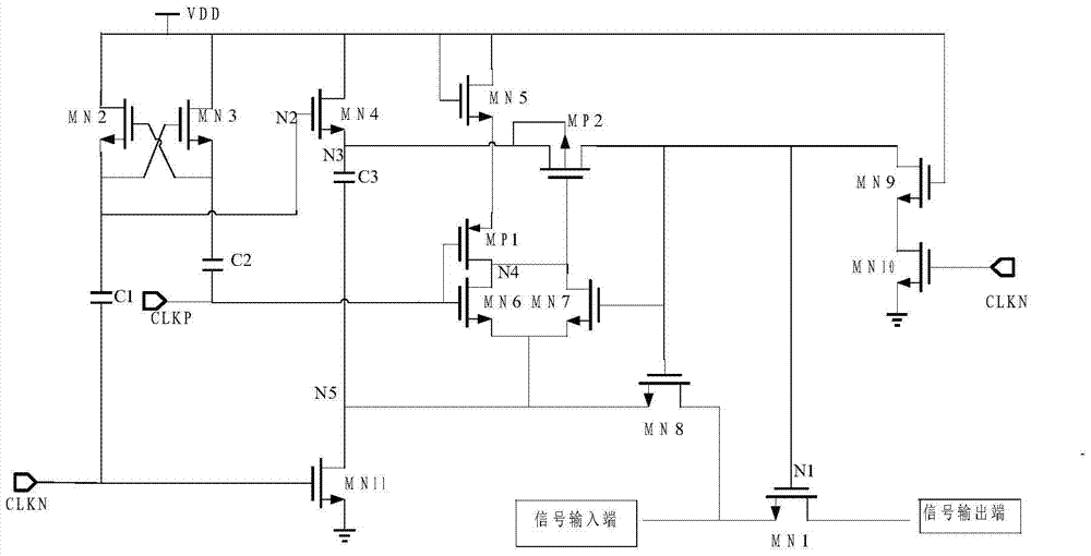
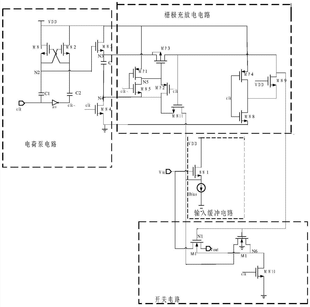
[0034] figure 2 It is a circuit diagram of a CMOS gate voltage bootstrap switch circuit according to an embodiment of the present invention. refer to figure 2 , the gate voltage bootstrap switch circuit in this example includes a charge pump circuit, a gate charge and discharge circuit, an input buffer circuit and a switch circuit, the charge pump circuit is connected to the gate charge and discharge circuit, the gate charge and discharge circuit is connected to the switch circuit, and the gate An input buffer circuit is connected between the charge and discharge circuit and the switch circuit. Wherein, the charge pump circuit is driven by the input buffer circuit, because the input buffer circuit isolates the input signal at the input terminal from the charge pump circuit, thereby greatly reducing the input parasitic capacitance. The charge pump circuit and the gate charging and discharging circuit constitute a gate voltage bootstrap loop, which is used to generate a gate...


PUM


Abstract

The present invention proposes a CMOS gate voltage bootstrap switch circuit, including a charge pump circuit, a gate charge and discharge circuit, an input buffer circuit and a switch circuit, the charge pump circuit is connected to the gate charge and discharge circuit, and the gate The pole charging and discharging circuit is connected to the switch circuit, and an input buffer circuit is connected between the gate charging and discharging circuit and the switching circuit. The invention uses the input buffer circuit to drive the charge pump circuit, because the input buffer circuit isolates the input signal at the input terminal and the charge pump circuit, thereby greatly reducing the input parasitic capacitance. Simultaneously, the present invention overcomes the non-linearity introduced by Vth variation caused by the lining bias effect which only realizes the constant gate-source voltage Vgs of the switching tube in the existing CMOS gate voltage bootstrap circuit.

Description

technical field [0001] The invention relates to the technical field of integrated circuits, in particular to a CMOS gate voltage bootstrap switch circuit. Background technique [0002] With the rapid development of semiconductor technology, high-speed and high-precision analog-to-digital converters have been widely used in digital communications, military radar and other fields. Pipelined ADC (Pipelined ADC), as one of the current mainstream ADC products, can well take into account the requirements of speed and precision. In the pipeline analog-to-digital converter, the digital-to-analog converter (MDAC) with multiplication is an important part, and its performance determines the performance of the entire pipeline analog-to-digital converter. With the shrinking of the process size, the switch circuit used in MDAC will undoubtedly face new challenges. For the switching circuit in the digital-to-analog converter with multiplication, it requires low on-resistance, small area,...

Claims


Application Information

Patent Timeline
Patent Type & Authority Patents(China)
IPC IPC(8): H03K17/687H03M1/12
Inventor 胡晨姚芹孙杰陈超吴建辉李红
Owner SOUTHEAST UNIV
Why Eureka
Try Eureka