Portable electronic device and integrated panel thereof
An electronic device and portable technology, applied in nonlinear optics, instruments, optics, etc., can solve the problems of a single virtual or mechanical key function in the virtual key area, and can not achieve diverse functions, so as to achieve the effect of differentiation
- Summary
- Abstract
- Description
- Claims
- Application Information
AI Technical Summary
Problems solved by technology
Method used
Image
Examples
no. 1 example
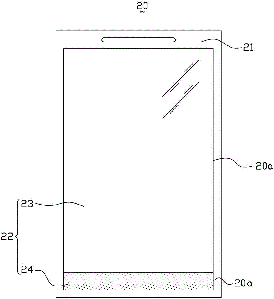
[0024] figure 2 For a schematic plan view of the portable electronic device in the embodiment of the present invention, please refer to figure 2 , the portable electronic device 20 of the embodiment of the present invention includes a module frame 21 and an integrated panel 22 assembled on the module frame 21 . In this embodiment, the portable electronic device 20 is, for example, a smart phone, a smart watch or a tablet computer. The portable electronic device 20 has a main display area 20a and a virtual key area 20b. The virtual key area 20b is located at the bottom of the portable electronic device 20, that is, the virtual key area 20b is located below the main display area 20a.
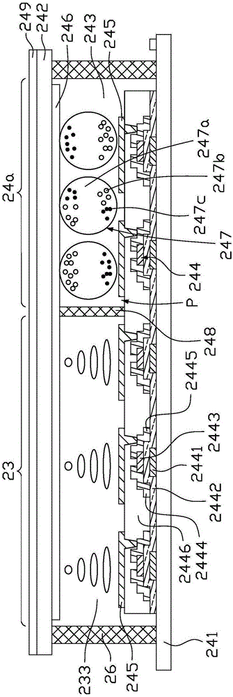
[0025] image 3 It is a schematic cross-sectional view of the integrated panel in the first embodiment of the present invention, please combine figure 2 and image 3 , the integrated panel 22 includes a main panel 23 and an electronic paper panel 24 located at the bottom of the main panel 2...
no. 2 example
[0044] Figure 4 It is a schematic cross-sectional view of the integrated panel in the second embodiment of the present invention, please refer to Figure 4 The difference between this embodiment and the above-mentioned first embodiment is that the electronic paper panel 24 is a cholesteric liquid crystal panel 24b.
[0045] In this embodiment, the cholesteric liquid crystal panel 24b includes a first substrate 241, a second substrate 242, and a cholesteric liquid crystal layer 250 sandwiched between the first substrate 241 and the second substrate 242. The first substrate 241 is provided with a plurality of thin film transistors 244 and a plurality of pixel electrodes 245 distributed in an array. The second substrate 242 is provided with a common electrode 246 , and the cholesteric liquid crystal layer 250 is provided with a cholesteric liquid crystal 251 .
[0046] Further, the first substrate 241 is further provided with a light-absorbing layer 252 , the light-absorbing l...
no. 3 example
[0054] Figure 5 It is a schematic cross-sectional view of the integrated panel in the third embodiment of the present invention, please refer to Figure 5 The difference between this embodiment and the above-mentioned first embodiment is that the electronic paper panel 24 and the main panel 23 are spliced and assembled together, that is, the electronic paper panel 24 and the main panel 23 are made separately and independently, and then spliced and assembled into an integrated panel 22.
[0055] By splicing and assembling, the electronic paper panel 24 can be manufactured independently of the main panel 23 , which has lower technical requirements compared with the above-mentioned first and second embodiments. By combining the two screens (the main panel 23 and the electronic paper panel 24), and then connecting to the circuit board (not shown) through a flexible circuit board (FPC, not shown), the electronic paper panel 24 can display the system's Some information to ena...
PUM
 Abstract
Description
Claims
Application Information


