
Patterned electrode manufacturing method, liquid crystal display panel and liquid crystal display panel manufacturing method

A liquid crystal display panel, patterned electrode technology, applied in the direction of circuits, electrical components, electrical solid devices, etc., can solve the problems of increased manufacturing process cost, high price of positive photoresist, and ITO application restrictions, so as to improve product competition force, achieve multi-domain vertical alignment, and reduce production costs

Inactive Publication Date: 2016-01-20
TCL CHINA STAR OPTOELECTRONICS TECH CO LTD
View PDF6 Cites 17 Cited by
  • Summary
  • Abstract
  • Description
  • Claims
  • Application Information

AI Technical Summary

Problems solved by technology

[0005] In the existing technology, PVD, CVD and other technologies are mainly used to make ITO thin films. Although these technologies are relatively mature, the production cost is relatively high.
At the same time, the metal indium in ITO is a rare metal. With the continuous consumption and rising price, the application of ITO in industry is limited.
In addition, when making ITO special pattern electrodes, due to high resolution requirements, positive photoresist coating is also required, and the price of positive photoresist is high, resulting in increased manufacturing process costs

Method used


Image

  • Patterned electrode manufacturing method, liquid crystal display panel and liquid crystal display panel manufacturing method
  • Patterned electrode manufacturing method, liquid crystal display panel and liquid crystal display panel manufacturing method
  • Patterned electrode manufacturing method, liquid crystal display panel and liquid crystal display panel manufacturing method

Examples


Embodiment Construction

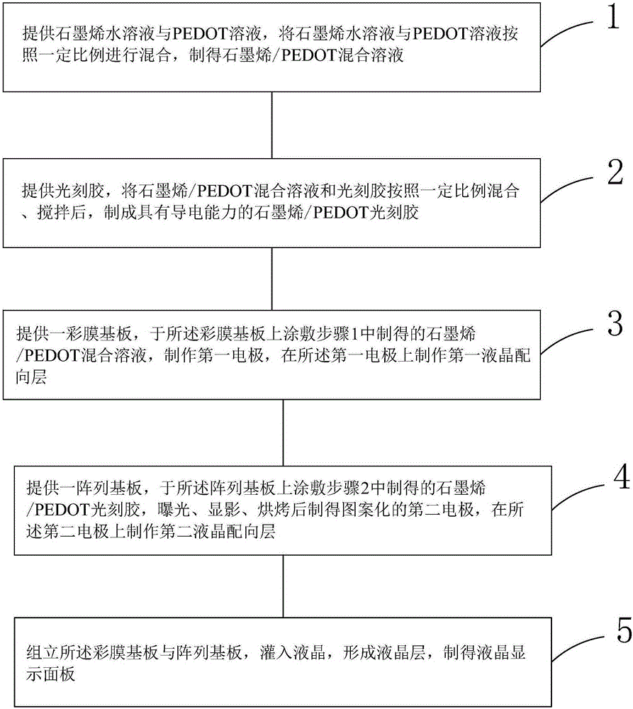
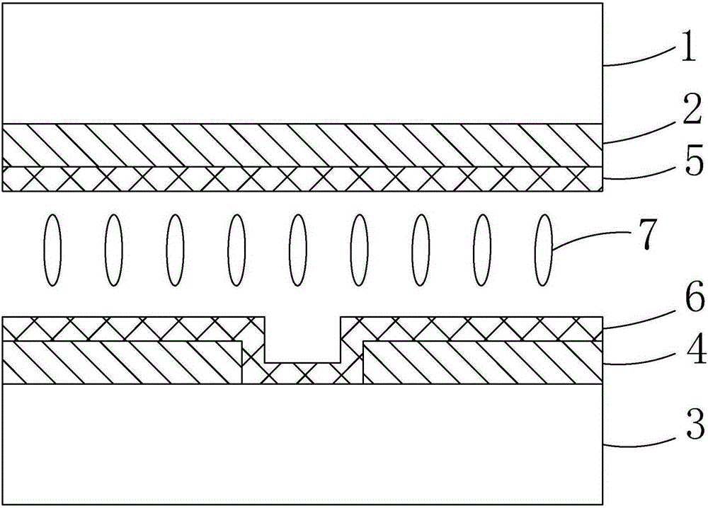
[0037] In order to further illustrate the technical means adopted by the present invention and its effects, the following describes in detail in conjunction with preferred embodiments of the present invention and accompanying drawings.

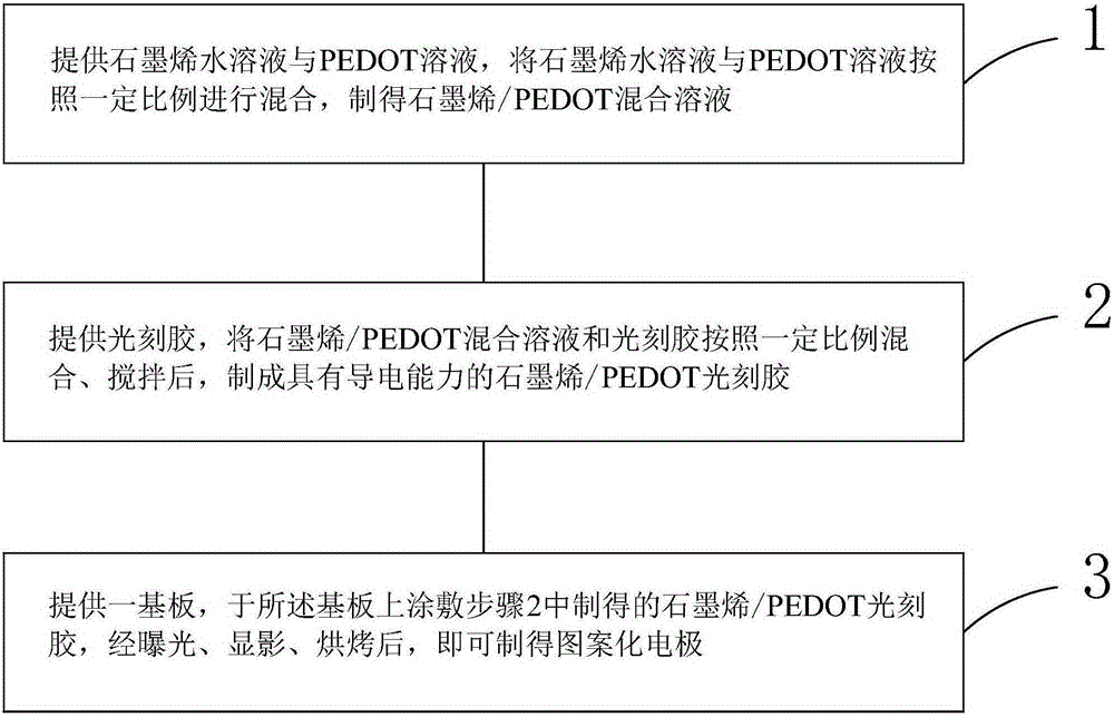
[0038] see figure 1 , the present invention firstly provides a method for fabricating a patterned electrode, comprising the following steps:

[0039] Step 1, provide graphene aqueous solution and PEDOT:PSS (poly(3,4-ethylenedioxythiophene)) solution, graphene aqueous solution and PEDOT:PSS solution are mixed according to a certain ratio, make graphene / PEDOT: PSS mixed solution.

[0040] Specifically, the mass percentage of graphene in the graphene aqueous solution is 1wt%-99wt%, preferably 50wt%.

[0041] Specifically, the mass percentage of PEDOT:PSS in the PEDOT:PSS solution is 1wt%-99wt%, preferably 50wt%.

[0042] Specifically, the graphene aqueous solution is mixed with the PEDOT:PSS solution at a mass ratio of 1:5-1:100; preferably, t...


PUM


Abstract

The invention provides a patterned electrode manufacturing method, a liquid crystal display panel and a liquid crystal display panel manufacturing method. The patterned electrode manufacturing method comprises the steps of 1, mixing a graphene aqueous solution with a PEDOT:PSS solution according to a certain proportion to obtain a graphene / PEDOT:PSS mixed solution; 2, mixing the graphene / PEDOT:PSS mixed solution with photoresist according to a certain proportion and conducting stirring to obtain graphene / PEDOT:PSS photoresist with conductivity; 3, providing a substrate, applying the graphene / PEDOT:PSS photoresist prepared in the step 2 onto the substrate, and conducting exposure, development and baking to obtain a patterned electrode. Compared with traditional ITO electrode manufacturing methods, the patterned electrode manufacturing method has the advantages that the patterned electrode manufacturing processes can be simplified, and patterned electrode manufacturing cost can be reduced.

Description

technical field [0001] The invention relates to the field of display technology, in particular to a method for manufacturing a patterned electrode, a liquid crystal display panel and a method for manufacturing the same. Background technique [0002] A liquid crystal display (Liquid Crystal Display, LCD) is one of the most widely used flat panel displays at present, and a liquid crystal display panel is a core component of the liquid crystal display. A liquid crystal display panel is usually composed of a color filter substrate (ColorFilter, CF), a thin film transistor array substrate (ThinFilmTransistorArraySubstrate, TFTArraySubstrate), and a liquid crystal layer (LiquidCrystalLayer) disposed between the two substrates. Generally, pixel electrodes and common electrodes are respectively arranged on the array substrate and the color filter substrate. When a voltage is applied to the pixel electrode and the common electrode, an electric field will be generated in the liquid c...

Claims


Application Information

Patent Timeline
Patent Type & Authority Applications(China)
IPC IPC(8): G02F1/1343G02F1/1333
CPCG02F1/1333G02F1/13439G02F2202/022H10K71/621H10K85/1135G02F2201/121G02F2201/123G02F2202/16G02F2203/01
Inventor 李泳锐王海军胡韬
Owner TCL CHINA STAR OPTOELECTRONICS TECH CO LTD
Learn More