Display panel
A display panel and substrate technology, applied in identification devices, nonlinear optics, instruments, etc., can solve problems such as easy residue of developer, difficulty in completely removing photoresist, and impact on display panel transmittance
- Summary
- Abstract
- Description
- Claims
- Application Information
AI Technical Summary
Problems solved by technology
Method used
Image

Examples
Embodiment Construction
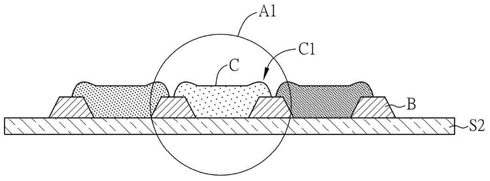
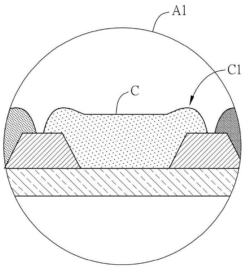
[0056] The structure of the display panel and the black matrix according to the preferred embodiment of the present invention will be described below with reference to the related drawings, wherein the same elements and components will be described with the same reference symbols. In addition, the illustrations of all the embodiments of the present invention are only schematic, and do not represent actual dimensions and proportions.
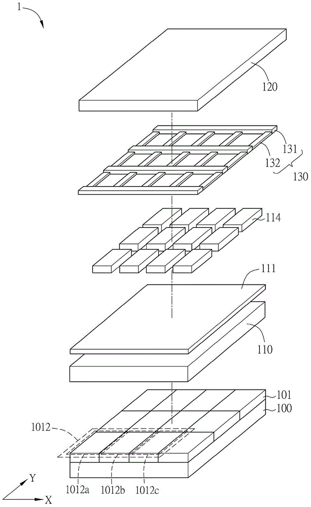
[0057] Please refer to Figure 2A as well as Figure 2B , the present invention can provide a display panel 1 , which can at least include a first substrate 100 , a second substrate 120 and a black matrix 130 . And the display panel 1 can further include a display medium 110 disposed between the first substrate 100 and the second substrate 120 . The display medium 110 can be, for example, a liquid crystal material, a plasma material, or an organic light-emitting material. Therefore, the display panel 1 can be a liquid crystal display panel, a p...
PUM
| Property | Measurement | Unit |
|---|---|---|
| Thickness | aaaaa | aaaaa |
| Thickness | aaaaa | aaaaa |
Abstract
Description
Claims
Application Information
 - R&D Engineer
- R&D Manager
- IP Professional
- Industry Leading Data Capabilities
- Powerful AI technology
- Patent DNA Extraction
Browse by: Latest US Patents, China's latest patents, Technical Efficacy Thesaurus, Application Domain, Technology Topic.
© 2024 PatSnap. All rights reserved.Legal|Privacy policy|Modern Slavery Act Transparency Statement|Sitemap