Stand-alone double-table and multi-station automatic printed circuit board (PCB) exposure equipment and exposure method

A PCB board and double-table technology, applied in the field of PCB board manufacturing, can solve the problems of low efficiency of manual operation, influence of PCB board production quality, high requirements for PCB board exposure, etc., achieve free placement, small trouble-free time, increase The effect of capacity

Inactive Publication Date: 2016-01-27
JIANGSU YSPHOTECH INTERGRATED CIRCUIT EQUIP CO LTD
View PDF12 Cites 5 Cited by
  • Summary
  • Abstract
  • Description
  • Claims
  • Application Information

AI Technical Summary

Problems solved by technology

[0002] During the production process of the PCB board, double-sided exposure is required, and there are special equipment for exposure. At present, the double-sided exposure of the PCB board is manually operated. First, one side of the PCB board is exposed, and then the PCB board is reversed to re-expose the PCB board. On the other side, PCB board exposure requirements are very high, and manual operation will inevitably cause board placement errors, which will have a certain impact on the production quality of PCB boards. In addition, manual operation is inefficient and the output is limited.

Method used


Image

  • Stand-alone double-table and multi-station automatic printed circuit board (PCB) exposure equipment and exposure method

Examples


Embodiment Construction

[0017] The present invention will be further described below in conjunction with accompanying drawing.

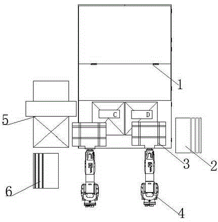
[0018] Such as figure 1 As shown, this single-machine double-table multi-station automatic PCB exposure equipment includes a PCB board cleaning machine 5, a PCB board exposure machine 1, two manipulators 4, a material bin 6 to be exposed and a material bin 2 after exposure; the two manipulators 4 are parallel Setting, the setting position of the PCB board exposure machine 1 corresponds to the position of the two manipulators 4, the PCB board cleaning machine 5 is set on the outside of one manipulator 4, and the material bin 6 to be exposed is set behind the PCB board cleaning machine 5; the exposure material bin 2 is completed It is arranged on the outside of another manipulator 4; in order to improve the working scope of the present invention, the manipulator 4 is provided with splint tooling 3; the manipulator 4 is a multi-dimensional manipulator.

[0019] The exposure m...


PUM


Abstract

The invention discloses a stand-alone double-table and multi-station automatic printed circuit board (PCB) exposure equipment and exposure method. The stand-alone double-table and multi-station automatic PCB exposure equipment comprises a PCB cleaning machine, a PCB exposure machine, two manipulators, a to-be-exposed stock bin and an exposed stock bin; and the exposure method comprises the following steps: (a) one manipulator puts a PCB on the PCB cleaning machine from the to-be-exposed stock bin; (b) the PCB is cleaned by the PCB cleaning machine; (c) after cleaning is ended, the manipulator puts the PCB on a first station for carrying out a front exposure on the PCB from the PCB cleaning machine; (d) after the exposure is ended, the manipulator takes out the PCB and transfers the PCB to the other manipulator; (e) the other manipulator puts the PCB on a second station for carrying out a reverse exposure on the PCB; and (f) after the exposure is ended, the other manipulator puts the PCB of which the front and reverse surfaces are exposed on the exposed stock bin. Cleaning and exposure of the PCB are operated by the manipulators, so that the efficiency is improved; the capacity is improved; a board putting error cause by human factors is reduced; the board putting accuracy is improved; the stability of the multi-dimensional manipulators is high; and the mean time to failure of a complete set of system is short.

Description

technical field [0001] The invention relates to a single-machine, double-table, multi-station automatic PCB board exposure equipment and an exposure method thereof, belonging to the PCB board manufacturing industry. Background technique [0002] During the production process of the PCB board, double-sided exposure is required, and there are special equipment for exposure. At present, the double-sided exposure of the PCB board is manually operated. First, one side of the PCB board is exposed, and then the PCB board is reversed to re-expose the PCB board. On the other hand, PCB board exposure requirements are very high, and manual manual operation will inevitably cause board placement errors, which will have a certain impact on the production quality of PCB boards. In addition, manual manual operation is inefficient and the output is limited. Contents of the invention [0003] Aiming at the above-mentioned problems in the prior art, the present invention provides a single-ma...

Claims


Application Information

Patent Timeline
Patent Type & Authority Applications(China)
IPC IPC(8): G03F7/20
Inventor 王小爱程珂赵华
Owner JIANGSU YSPHOTECH INTERGRATED CIRCUIT EQUIP CO LTD
Why Eureka
Try Eureka