
A method for reading nand Flash parameters

A parameter reading and parameter technology, applied in the field of reading NandFlash parameters, can solve the problem of inability to operate different types of NandFlash correctly.

Active Publication Date: 2018-02-13
TANGRAM MICROELECTRONICS TECH SHANGHAI CO LTD
View PDF4 Cites 0 Cited by
  • Summary
  • Abstract
  • Description
  • Claims
  • Application Information

AI Technical Summary

Problems solved by technology

It can solve the problem that a piece of solidified code cannot correctly operate different types of Nand Flash

Method used


Image

  • A method for reading nand Flash parameters
  • A method for reading nand Flash parameters
  • A method for reading nand Flash parameters

Examples


Embodiment Construction

[0021] In order to make the objectives, technical solutions, and advantages of the embodiments of the present invention clearer, the technical solutions in the embodiments of the present invention will be described clearly and completely in conjunction with the accompanying drawings in the embodiments of the present invention. Obviously, the described embodiments It is a part of the embodiments of the present invention, not all the embodiments. Based on the embodiments of the present invention, all other embodiments obtained by those of ordinary skill in the art without creative work shall fall within the protection scope of the present invention.

[0022] In order to facilitate the understanding of the embodiments of the present invention, further explanations will be made below with specific embodiments in conjunction with the drawings.

[0023] In view of the fact that the existing Nand Flash parameters can only be specified at compile time or selected through the pin configurat...


PUM


Abstract

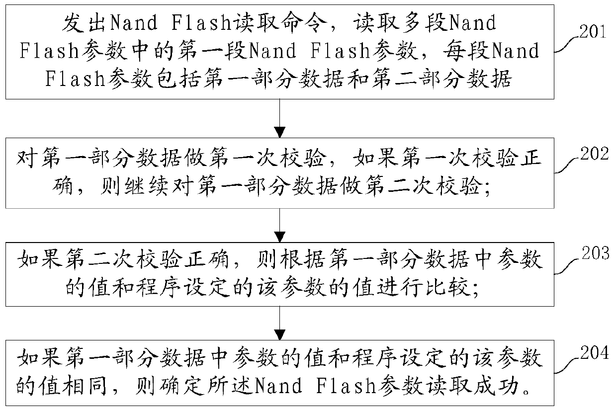
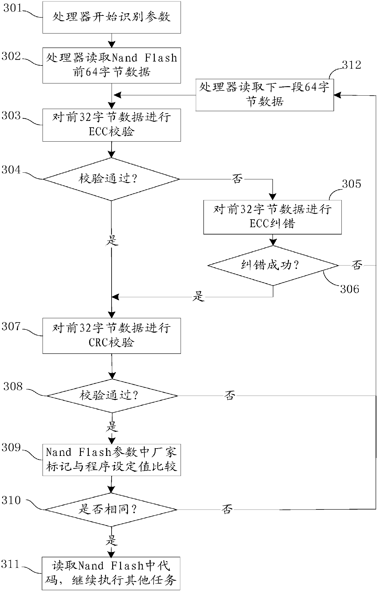
The invention relates to a Nand Flash parameter reading method. The method includes the following steps that a Nand Flash reading command is sent, and a first section of Nand Flash parameters in multiple sections of Nand Flash parameters are read, wherein each section of Nand Flash parameters includes a first part of data and a second part of data; the first part of data are verified for the first time, and if verified to be corrected in the first time of verification, the first part of data continue to be verified for the second time; if the first part of data are verified to be corrected in the second time of verification, values of parameters in the first part of data are compared with values set by a program; if the values of the parameters in the first part of data and the values set by the program are the same, it is determined that Nand Flash parameter reading succeeds. Through the method, automatic identification of Nand Flash parameters is achieved without adding memorizers or increasing cost.

Description

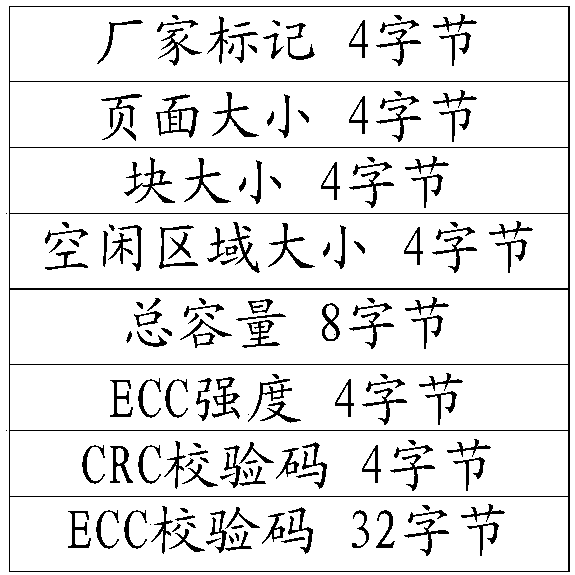
Technical field [0001] The present invention relates to the field of semiconductor technology, in particular to a method for reading Nand Flash parameters. Background technique [0002] As a low-cost, large-capacity storage device, Nand Flash is used more and more widely in embedded systems. Different models of Nand Flash have different page sizes, block sizes, and free area sizes, and different NandFlash has different ECC check strengths. In Nand Flash chips that do not support the ONFI (Open Nand Flash Interface) standard protocol, These data can only be obtained through the data manual provided by the manufacturer. [0003] In embedded applications that use Nand Flash as a storage device, after the processor is reset, it will first execute a code called ROM code that is solidified inside the processor chip, and read the code from Nand Flash to the on-chip or off-chip RAM , And then run the corresponding program. To correctly read the code from Nand Flash, you must first obtai...

Claims


Application Information

Patent Timeline
Patent Type & Authority Patents(China)
IPC IPC(8): G11C29/42
Inventor 谢长武卜弋天庹凌云刘方李烨
Owner TANGRAM MICROELECTRONICS TECH SHANGHAI CO LTD
Learn More