Eureka AIR delivers breakthrough ideas for toughest innovation challenges, trusted by R&D personnel around the world.

Array substrate and manufacturing method thereof, display panel and display device

A technology for array substrates and display panels, applied in semiconductor/solid-state device manufacturing, electrical components, electric solid-state devices, etc.

Active Publication Date: 2018-06-15
BOE TECH GRP CO LTD +1
View PDF3 Cites 0 Cited by
  • Summary
  • Abstract
  • Description
  • Claims
  • Application Information

AI Technical Summary

Problems solved by technology

[0005] figure 1 In the array substrate, in order to ensure the power supply capability of the common electrode wiring 230, the width of the common electrode wiring 230 should not be too small, which limits the narrowing of the display device.

Method used


Image

  • Array substrate and manufacturing method thereof, display panel and display device
  • Array substrate and manufacturing method thereof, display panel and display device
  • Array substrate and manufacturing method thereof, display panel and display device

Examples


Embodiment 1

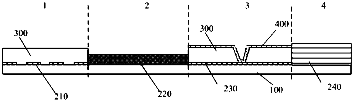
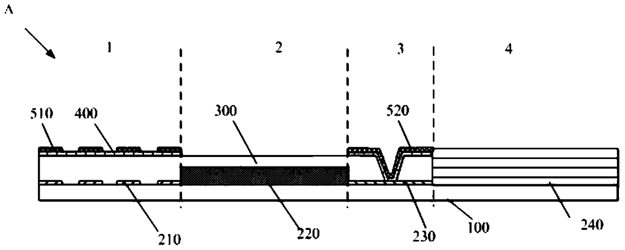
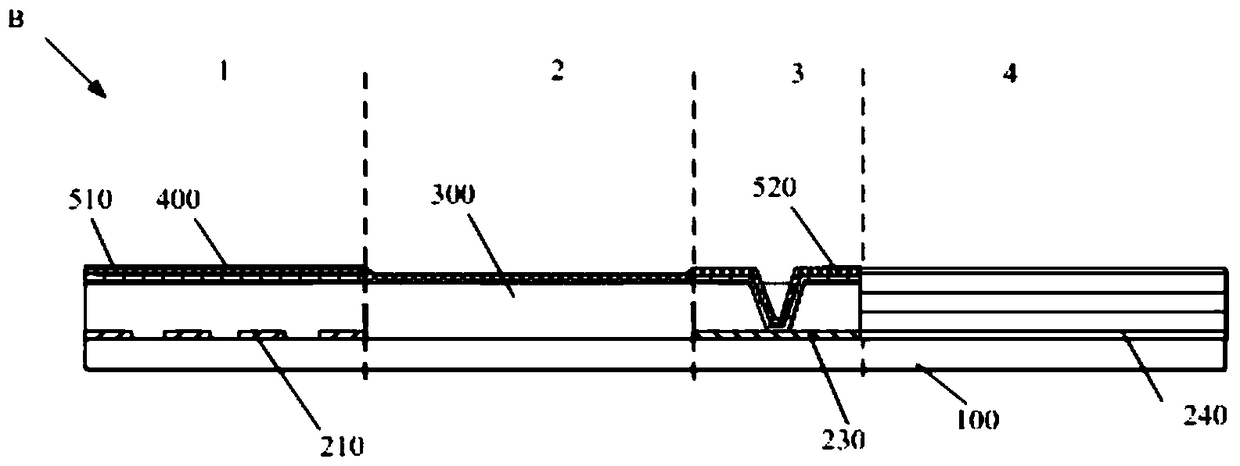
[0055] For the array substrate provided in Embodiment 1 of the present invention, please refer to figure 2 , image 3 and Figure 4 ,in figure 2 for in Figure 4 The schematic cross-sectional view at A shown in, image 3 for in Figure 4 The schematic cross-sectional view at B shown in ; the array substrate includes: a substrate 100, which can be divided into four regions 1, 2, 3, and 4 according to the structure formed above the substrate 100; specifically, Area 1 is a GOA signal line area, and the array substrate has a GOA signal line 210 on the base 100 in this area; Area 2 is a GOA area, and the array substrate has a GOA circuit 220 on the base 100 in this area, see Figure 4 , the GOA circuit 220 includes a plurality of shift register units 221 cascaded together, and each shift register unit 221 includes a plurality of thin film transistors (not shown); area 3 is the common electrode wiring (COM) area, the array substrate has a first common electrode wiring 230 on...

Embodiment 2

[0072] The structure of the array substrate provided by Embodiment 2 of the present invention may refer to Figure 5 , Image 6 and Figure 7 ,in Figure 5 for in Figure 7 The schematic cross-sectional view at A shown in, Image 6 for in Figure 7The schematic cross-sectional view at B shown in ; in Embodiment 2 of the present invention, the gate drive circuit trace 210, the gate drive circuit 220, the first common electrode trace 230, the second common electrode trace 510, and the conductive connection part 520 is also provided with an insulating layer 300, the insulating layer 300 is provided with a via hole at the position of the first common electrode trace 230, the first common electrode trace 230 and the conductive connection part 520 are connected through the via hole; Figure 2-Figure 4 The structure of the array substrate is different in that the gate driving circuit wiring 210 , the gate driving circuit 220 and the first common electrode wiring 230 are located ...


PUM


Abstract

The invention provides an array substrate and a manufacturing method thereof, a display panel, and a display device. The array substrate includes insulating layers, a second common electrode line formed in the line area of a gate drive circuit, a conductive connection part formed in the gate drive circuit area and a first common electrode line area, the second common electrode line is connected with the conductive connection part, the insulating layers are arranged between the second common electrode line and the gate drive circuit line, between the conductive connection part and the gate drive circuit, and between the conductive connection part and the first common electrode line, the insulating layer between the conductive connection part and the first common electrode line is provided with a through hole, and the conductive connection part is connected with the first common electrode line via the through hole. The array substrate facilitates the edge narrowing of the corresponding display device.

Description

technical field [0001] The present invention relates to the field of display technology, in particular to an array substrate and a manufacturing method thereof, a display panel and a display device. Background technique [0002] GOA ((Gate Driver On Array, gate drive circuit on the array substrate) [0003] Technology Compared with traditional Chip On Flex / Film (COF) and directly bonded on glass (Chip OnGlass, COG) processes, GOA technology can not only save costs, but also the panel can achieve a symmetrical and beautiful design on both sides. The main feature of the technology is that it relies on the continuous triggering of the GOA unit to realize its shift register function, which saves the bonding (Bonding) area of ​​the gate integrated circuit (GateIC) and the Fan-out wiring space, and realizes the design of a narrow frame; at the same time, due to The Bonding process in the Gate direction can be omitted, which is also beneficial to the improvement of production capa...

Claims


Application Information

Patent Timeline
Patent Type & Authority Patents(China)
IPC IPC(8): H01L27/12H01L21/77
Inventor 廖力勍李红敏
Owner BOE TECH GRP CO LTD
Why Eureka
Eureka Blog
Learn More