Dispatching optimization method for electroless copper plating process of multiple layers of circuit boards

A process and optimization scheduling technology, applied in the direction of total factory control, total factory control, electrical program control, etc., can solve the heuristic constructive method to optimize poor quality, multi-layer circuit board chemical copper plating process scheduling problem NP Difficulty and other issues

Inactive Publication Date: 2014-07-23
KUNMING UNIV OF SCI & TECH
View PDF2 Cites 9 Cited by
  • Summary
  • Abstract
  • Description
  • Claims
  • Application Information

AI Technical Summary

Problems solved by technology

[0004] Since the process scheduling problem of electroless copper plating process of multilayer circuit board is NP-hard, the traditional ma

Method used


Image

  • Dispatching optimization method for electroless copper plating process of multiple layers of circuit boards
  • Dispatching optimization method for electroless copper plating process of multiple layers of circuit boards
  • Dispatching optimization method for electroless copper plating process of multiple layers of circuit boards

Examples


Embodiment 1

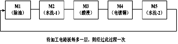
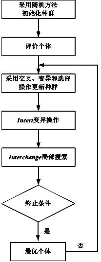
[0039] Embodiment 1: as Figure 1-5 As shown, an optimal scheduling method for the electroless copper plating process of a multi-layer circuit board, by determining the scheduling model and the optimization target of the electroless copper plating process, and using the optimal scheduling method based on the differential evolution algorithm to optimize the optimization target; The scheduling model is established according to the processing completion time of each circuit board on each process equipment, and the optimization goal is to minimize the earliest completion time C max :

[0040]

[0041] In the formula: m 5 sets of process equipment representing the copper plating process, Sum R means all n The sum of layers of circuit boards to be processed, n Indicates the number of circuit boards to be processed, is the process sequence of circuit boards to be processed, ( j =1,..., Sum R ) means sorting π B j position of the circuit board, Indicates the circuit ...

Embodiment 2

[0050] Embodiment 2: as Figure 1-5 As shown, an optimal scheduling method for the electroless copper plating process of a multi-layer circuit board, by determining the scheduling model and the optimization target of the electroless copper plating process, and using the optimal scheduling method based on the differential evolution algorithm to optimize the optimization target; The scheduling model is established according to the processing completion time of each circuit board on each process equipment, and the optimization goal is to minimize the earliest completion time C max :

[0051]

[0052] In the formula: m 5 sets of process equipment representing the copper plating process, Sum R means all n The sum of the layers of each circuit board to be processed (the number of layers of copper plating required for each circuit board is not the same), n Indicates the number of circuit boards to be processed, is the process sequence of circuit boards to be processed, ( ...


PUM


Abstract

The invention relates to a dispatching optimization method for the electroless copper plating process of multiple layers of circuit boards and belongs to the technical field of intelligent dispatching optimization in a production workshop. The dispatching optimization method comprises the steps that a dispatching model and an optimization objective of the electroless copper plating process are determined, and the optimization objective is optimized through a dispatching optimization method based on the differential evolution algorithm; the dispatching model is established according to processing finishing time of each circuit board on each process device, and meanwhile the optimization objective is obtained by minimizing the earliest finishing time. By means of the dispatching optimization method, the algorithm can be better guided to conduct global search; historical information of superior individuals can be fully utilized, and it can also be guaranteed that the global search of the algorithm has a certain width; as a result, the search field of the algorithm is wider, the local development capability of the algorithm is remarkably improved, and the solving quality is remarkably improved.

Description

technical field [0001] The invention relates to an optimal scheduling method for the chemical copper plating process of a multilayer circuit board, and belongs to the technical field of intelligent optimal scheduling of production workshops. Background technique [0002] Printed Circuit Board (PCB) is the carrier for the integration of electronic components and one of the most important components in the electronics industry. Almost every kind of electrical equipment uses printed boards in order to realize the electrical interconnection between different components. In terms of PCB product structure, multilayer circuit boards account for most of the output value, and the manufacturing capacity of multilayer circuit boards has become the most important standard for measuring the technical level of the PCB industry. With the increasingly fierce market competition, how to effectively improve the efficiency of each link in the production process of multilayer circuit boards is ...

Claims


Application Information

Patent Timeline
IPC IPC(8): G05B19/418
CPCY02P90/02
Inventor 钱斌万婧胡蓉
Owner KUNMING UNIV OF SCI & TECH
Why Eureka
Try Eureka