Supercharge Your Innovation With Domain-Expert AI Agents!

Time Domain Simulation Circuit and Simulation Method of Pin Diode

A PIN diode, time-domain simulation technology, applied in the direction of electrical digital data processing, special data processing applications, instruments, etc., can solve the problem that the transient response characteristics of PIN limiting diodes cannot be simulated, and achieve the effect of simple simulation method

Active Publication Date: 2016-12-07
CHINA SHIP DEV & DESIGN CENT
View PDF2 Cites 0 Cited by
  • Summary
  • Abstract
  • Description
  • Claims
  • Application Information

AI Technical Summary

Problems solved by technology

[0003] The purpose of the present invention is to provide a time-domain simulation circuit and simulation method of a PIN diode, which can solve the problem that the general diode simulation model in the existing circuit-level electromagnetic simulation commercial software cannot simulate the PIN limiter diode in the electromagnetic pulse Problems with transient response characteristics under action

Method used


Image

  • Time Domain Simulation Circuit and Simulation Method of Pin Diode
  • Time Domain Simulation Circuit and Simulation Method of Pin Diode
  • Time Domain Simulation Circuit and Simulation Method of Pin Diode

Examples


Embodiment Construction

[0041] In order to make the object, technical solution and advantages of the present invention clearer, the present invention will be further described in detail below in conjunction with the accompanying drawings and embodiments. It should be understood that the specific embodiments described here are only used to explain the present invention, not to limit the present invention.

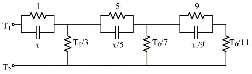
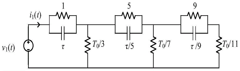
[0042] see Figure 9 , a time-domain simulation circuit of a PIN diode, comprising four sub-circuits;

[0043] Sub-circuit 1 describes the PIN diode junction capacitance, packaging capacitance and lead inductance; Sub-circuit 1 also includes the series structure of PIN diode dies, including I-layer equivalent circuit and PN junction equivalent circuit; Sub-circuit 2 and Sub-circuit 3 Combined with the PN junction equivalent circuit in subcircuit 1, it jointly describes the relationship between the PIN diode current and the PN junction voltage drop; the combination of subcircuit 4 and the I-layer e...


PUM


Abstract

The invention discloses a PIN diode time domain equivalent circuit model. The model comprises four sub-circuits, wherein the first sub-circuit describes an I-layer equivalent circuit and a PN junction equivalent circuit, the second sub-circuit and the third sub-circuit are combined with the PN junction equivalent circuit in the first sub-circuit to describe the relation between PIN diode current and PN junction voltage drop together, and the fourth sub-circuit is combined with the I-layer equivalent circuit in the first sub-circuit to describe the relation between PIN diode current and I-layer voltage drop. The invention further provides a modeling method of the PIN diode time domain equivalent circuit model. The PIN diode time domain transient equivalent circuit model can be established to reflect the peak leakage and recovery time of the charge-storage effect so as to precisely predict the time-domain response characteristics of a PIN diode under the action of various signals, and then a method is provided for predicting the electromagnetic pulse effect of the radio frequency front end of sensitive electronic information equipment.

Description

technical field [0001] The invention belongs to the simulation field of semiconductor devices, and in particular relates to a time-domain simulation circuit and simulation method of a PIN diode. Background technique [0002] When the radio frequency and microwave sensitive electronic information system is exposed to the electromagnetic pulse radiation field, the filter module, limiter module and low noise amplifier module in the receiving channel will be impacted by the electromagnetic pulse energy. According to the current electromagnetic pulse radiation field level, it is necessary to focus on the performance of the limiter module, because the time domain response characteristics (such as start-up time and leakage level) of the limiter module when the electromagnetic pulse is injected determines whether the receiving channel will be damaged or how disturbed it is. In order to predict these effects, reliable simulation models need to be established. The difficulty in the ...

Claims


Application Information

Patent Timeline
Patent Type & Authority Patents(China)
IPC IPC(8): G06F17/50
Inventor 王冬冬邓峰张崎高岚
Owner CHINA SHIP DEV & DESIGN CENT
Features
  • R&D
  • Intellectual Property
  • Life Sciences
  • Materials
  • Tech Scout
  • Unparalleled Data Quality
  • Higher Quality Content
  • 60% Fewer Hallucinations
Learn More