
Circuit and method for achieving two keys on single PAD

A button and circuit technology, which is applied in the field of integrated circuit input control, can solve the problems of increased chip packaging cost, unsolvable error identification, increased chip cost, etc., to reduce the area of ​​pins and packaging, avoid the problem of key strings, and save Effects of PAD resources

Active Publication Date: 2016-02-17
SHENZHEN YSPRING TECH
View PDF6 Cites 1 Cited by
  • Summary
  • Abstract
  • Description
  • Claims
  • Application Information

AI Technical Summary

Problems solved by technology

A single PAD realizes one button technology. If there are N buttons, N PADs are needed. The size of the PAD cannot be reduced with the upgrading of the process. Under this technology, if there are more buttons, the chip area will inevitably increase. At the same time, the number of bonded pins also increases, and the packaging area increases, which not only increases the cost of the chip and packaging, but also has great limitations in the application of the chip.
Multi-PAD is to realize matrix scanning buttons, which effectively solves the problems existing in single-pad technology to realize one button, but at the same time brings new problems, if there are three buttons or four buttons on any two lines scanned by row and column There may be a key error, which is what we often call string keys. This kind of error recognition cannot be solved by software or hardware.
[0006] To sum up, if a single PAD is used to implement a button, N buttons need N PADs, and the PAD area is relatively large, which will cause the chip area to be enlarged by the PAD and increase the chip cost.
If multi-PAD is used to realize matrix scanning, there will be a problem of string keys (unable to recognize real keys) if three keys appear on any two lines of row and column scanning; and PAD resources cannot be saved below 18 keys, but currently large The keys of some application products are less than ten keys

Method used


Image

  • Circuit and method for achieving two keys on single PAD
  • Circuit and method for achieving two keys on single PAD
  • Circuit and method for achieving two keys on single PAD

Examples


Embodiment Construction

[0026] It should be noted that, in the case of no conflict, the embodiments in the present application and the features in the embodiments can be combined with each other.

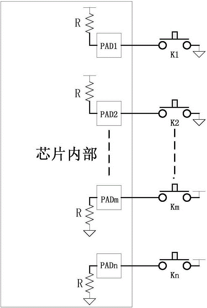
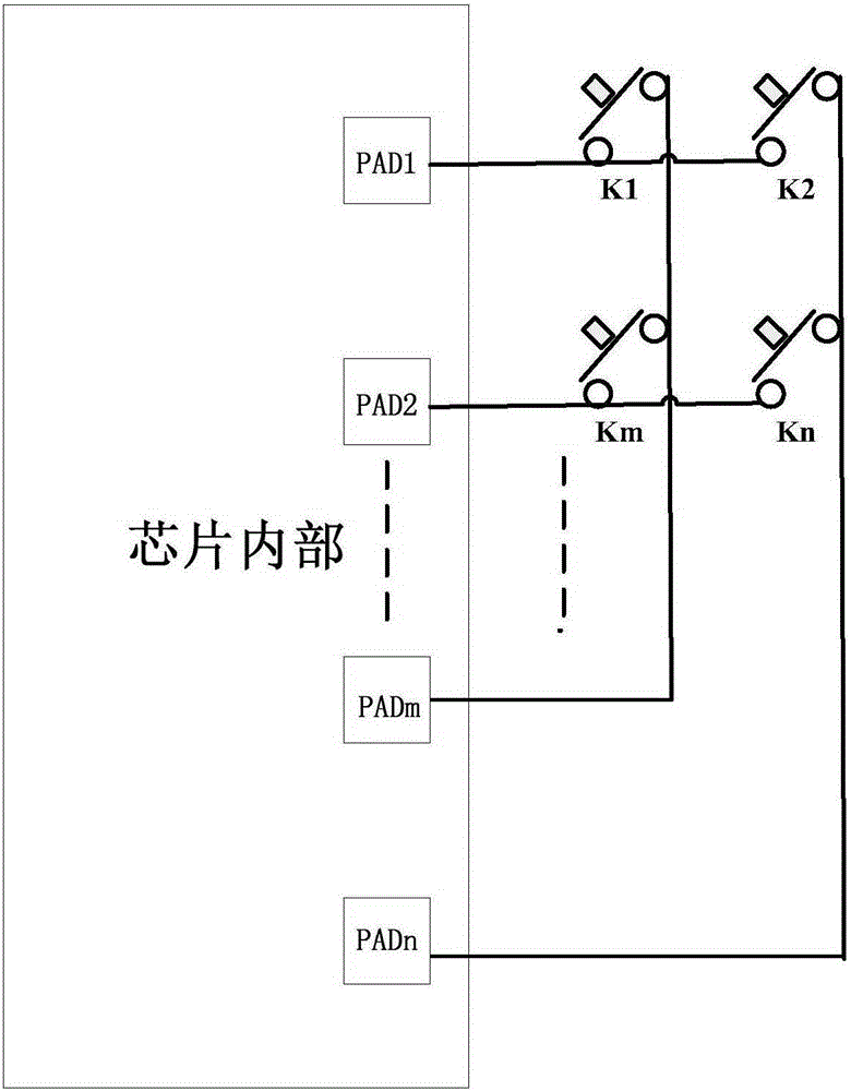
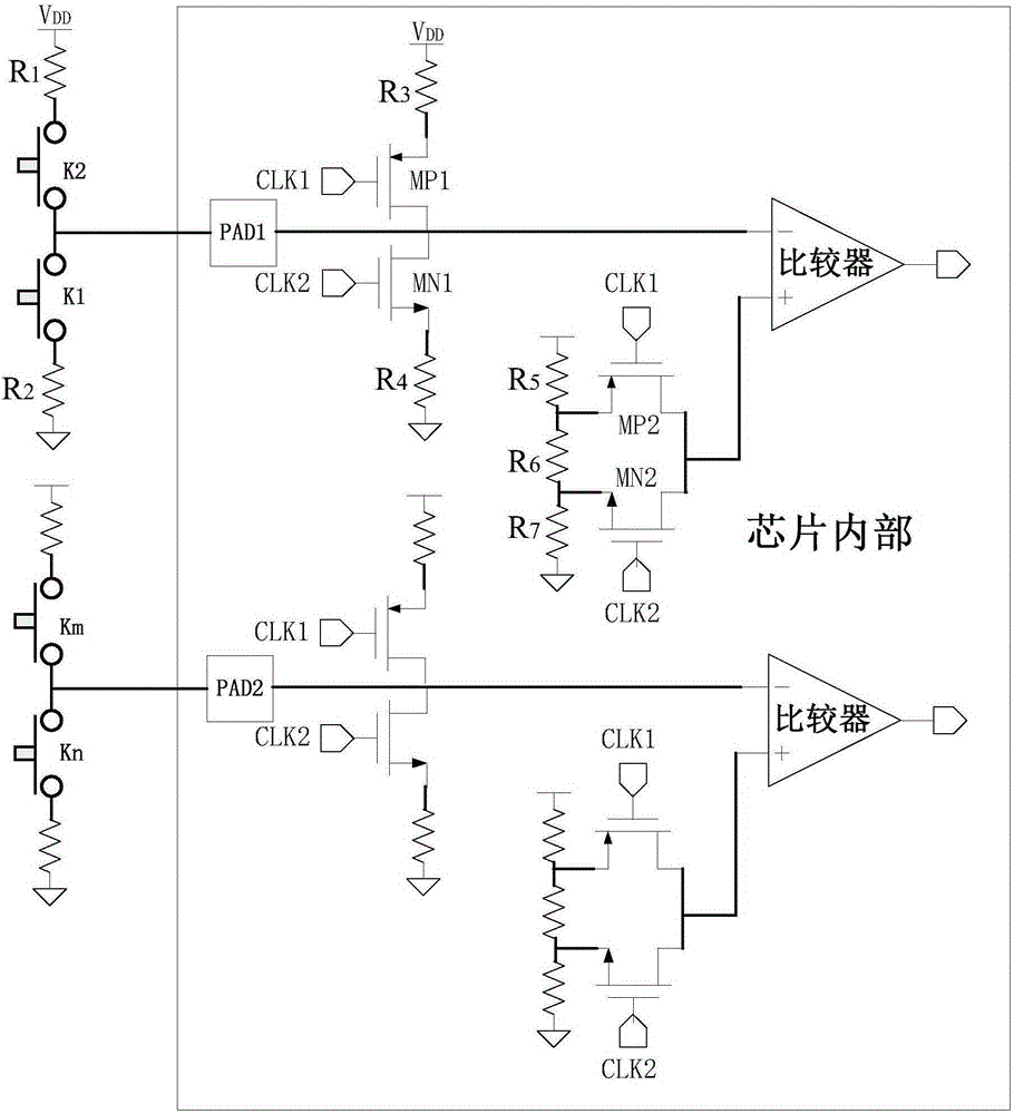
[0027] Such as image 3 As shown, a single PAD circuit realizes two buttons, which includes a first button K1, a second button K2, PAD pins PAD1 / PAD2, a first button sampling circuit, a second button sampling circuit, a reference voltage, a comparator And button identification circuit (not shown in the figure); one end of the first button K1 is connected to the PAD pin PAD1, and the other end is connected to the power supply VDD through the first resistor R1; one end of the second button K2 is connected to the PAD pin PAD1 , and the other end is grounded through the second resistor R2; the output ends of the sampling circuit of the first button K1 and the sampling circuit of the second button K2 are connected with the PAD pin PAD1, and are used for discontinuously testing the first button K1 and the second...


PUM


Abstract

The invention discloses a circuit and method for achieving two keys on a single PAD. The circuit comprises a first key, a second key, a PAD pin, a first key sampling circuit, a second key sampling circuit, a reference voltage device, a comparator and a key identification circuit, wherein one end of the first key is connected with the PAD pin and the other end is connected with a power source by a first resistor; one end of the second key is connected with the PAD pin and the other end is grounded via a second resistor; the output ends of the first and second key sampling circuits are connected with the PAD pin; and the first and second key sampling circuits are used for sampling the signals of the first and second keys according to the sequence signal interval. The circuit has the beneficial effects that two external keys are achieved on the single PAD through sampling control of the keys, thus avoiding the problem of key aliasing while saving the chip resources; and the circuit can be widely applied to keying circuit systems.

Description

technical field [0001] The invention relates to the field of integrated circuit input control, in particular to a circuit and method for realizing two buttons with a single PAD. Background technique [0002] PAD: chip pin. [0003] With the development of semiconductor integrated circuits, the technology used in integrated circuit chips is becoming more and more advanced, and the internal circuit integration of the chip is very high. This requires current chip products to reduce or reuse PAD as much as possible. Especially for application-type chip products, the area of ​​the chip accounts for the main part of the cost of the chip, and reducing the chip area can also achieve the effect of improving the competitiveness of the chip. [0004] In the prior art, chip button applications are divided into two types: a single PAD realizes a button; multi-PAD realizes a matrix scanning button. [0005] Such as figure 1 As shown, a single PAD realizes one button; figure 2 As sho...

Claims


Application Information

Patent Timeline
IPC IPC(8): H03K17/967
Inventor 肖永贵曾德智
Owner SHENZHEN YSPRING TECH
Features
  • Generate Ideas
  • Intellectual Property
  • Life Sciences
  • Materials
  • Tech Scout
  • Unparalleled Data Quality
  • Higher Quality Content
  • 60% Fewer Hallucinations
Learn More