Detection method for glue residue on hole wall of PCB

A technology of PCB board and detection method, which is applied in electrical components, printed circuit manufacturing, printed circuit and other directions, can solve the problems of high cost PCB board promotion and use, and achieve the effect of easy operation, simple detection process and cost reduction

Inactive Publication Date: 2016-02-24
CHONGQING FOUNDER HI TECH ELECTRONICS +1
View PDF3 Cites 3 Cited by
  • Summary
  • Abstract
  • Description
  • Claims
  • Application Information

AI Technical Summary

Problems solved by technology

[0006] The technical problem to be solved by the present invention is to overcome the defects of high cost and difficult to popularize and use in the PCB board preparation process of the prior art

Method used


Image

  • Detection method for glue residue on hole wall of PCB
  • Detection method for glue residue on hole wall of PCB
  • Detection method for glue residue on hole wall of PCB

Examples


Example Embodiment

[0038] Example 1

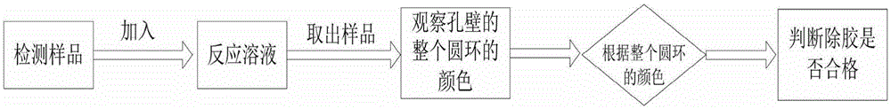
[0039] This embodiment provides a method for detecting glue slag on the hole wall of a PCB board, such as figure 1 shown, including the following steps:

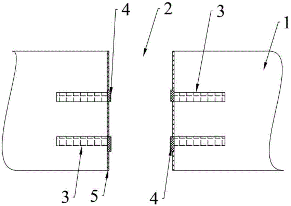
[0040] Putting the detection sample into a solution that can undergo a displacement reaction with the copper film 5 on the hole wall 2, so that the copper and the solution undergo a displacement reaction;

[0041] Observe the entire ring of the hole wall 2 at the position of the inner circuit 3 of the PCB board 1;

[0042] According to the color of the entire ring of hole wall 2, it is judged whether the glue removal is qualified;

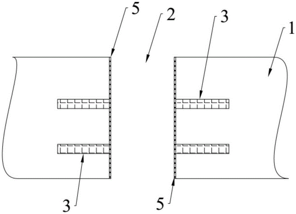
[0043] The test sample is the hole of the PCB board 1 with the copper film 5 deposited on the hole wall 2 .

[0044] The detection method of the slag 4 on the hole wall 2 of this embodiment only needs to put the detection sample into the solution that can undergo a displacement reaction with copper, and after the reaction is complete, the inner layer circuit of the PCB board...


PUM


Abstract

The invention discloses a detection method for a glue residue on the hole wall of a PCB. The detection method comprises the following steps: putting a detection sample in a solution capable of carrying out a replacement reaction with a copper film on the hole wall so that the replacement reaction of copper and the solution is carried out; observing the whole circular ring of the hole wall at the position of an inner-layer circuit of the PCB; judging whether glue removal is qualified according to the color of the whole circular ring of the hole wall, wherein the detection sample is the hole of the PCB deposited with the copper film on the hole wall. According to the detection method, as long as the detection sample is put in the solution capable of carrying out the replacement solution with the copper, the color of the whole circular ring of the hole wall at the position of the inner-layer circuit of the PCB can be intuitively observed after the reaction is completed so as to judge whether the glue removal is qualified, and an expensive fluorescence detector adopted in the prior art is not needed, so that the cost for detecting the glue residue on the hole wall is reduced, and the detection method is simple in detection process and easy in operation and can be widely popularized and applied in the preparation technology of PCB.

Description

technical field [0001] The invention relates to the technical field of detection of PCB boards, in particular to a detection method for glue slag on the hole wall of the PCB board. Background technique [0002] With the continuous development of PCB boards, the application of multi-layer structure PCB boards is becoming more and more extensive. With the increase of the number of PCB board layers, it is becoming more and more difficult to remove the glue residue on the hole wall after drilling holes on the PCB board. , because during the drilling process, the substrate material in the hole is melted at high temperature to form slag, a part of the slag is taken out of the hole by the drill bit, and the other part of the slag remains on the hole wall. Therefore, in the PCB board preparation process, all It is necessary to remove the glue on the hole wall after drilling, and test the degree of glue removal to judge whether the glue removal on the hole wall is qualified. If the ...

Claims


Application Information

Patent Timeline
IPC IPC(8): H05K3/00
CPCH05K3/00H05K2203/161
Inventor 马建李小晓
Owner CHONGQING FOUNDER HI TECH ELECTRONICS
Why Eureka
Try Eureka