Circuit board hole drilling method

A drilling method and circuit board technology, applied in printed circuits, printed circuit manufacturing, electrical components, etc., can solve problems such as low production efficiency of circuit boards, reduce drill bit swing, reduce adjustment time, and improve utilization rate. Effect

Inactive Publication Date: 2016-03-16
PEKING UNIV FOUNDER GRP CO LTD +1
View PDF7 Cites 10 Cited by
  • Summary
  • Abstract
  • Description
  • Claims
  • Application Information

AI Technical Summary

Problems solved by technology

[0005] Therefore, the technical problem to be solved by the present invention is that the circuit board production efficiency in the prior art is low

Method used


Image

  • Circuit board hole drilling method
  • Circuit board hole drilling method
  • Circuit board hole drilling method

Examples


Embodiment 1

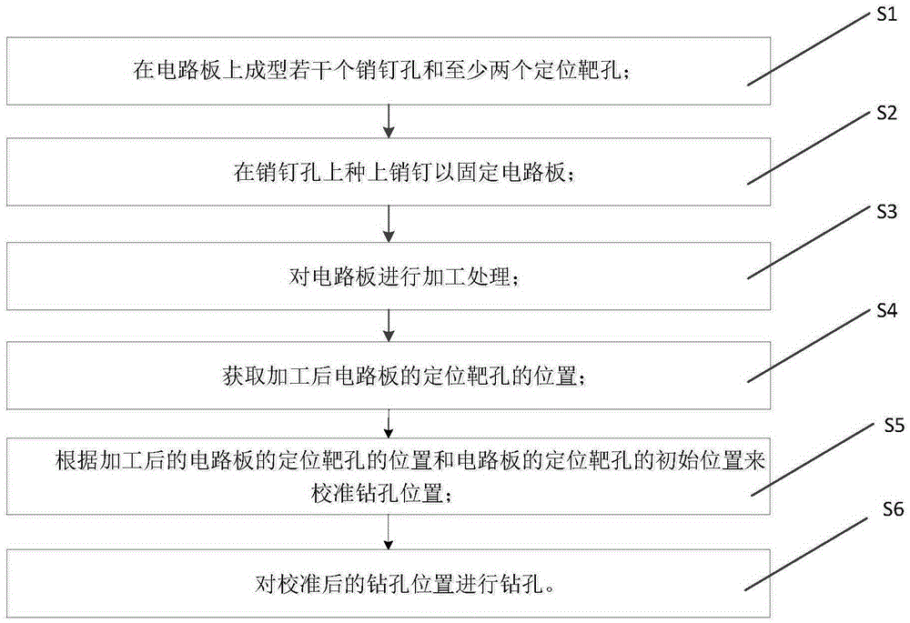
[0048] This embodiment provides a circuit board drilling method, such as figure 1 shown, including the following steps,

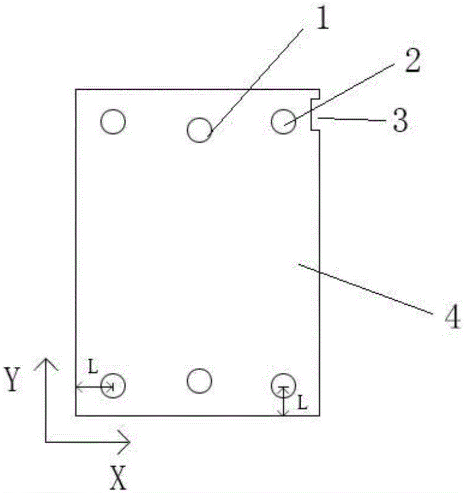
[0049] S1: forming several pin holes 1 and at least two positioning target holes 2 on the circuit board, see figure 2 ;

[0050] S2: Plant a pin on the pin hole 1 to fix the circuit board;

[0051] S3: process the circuit board;

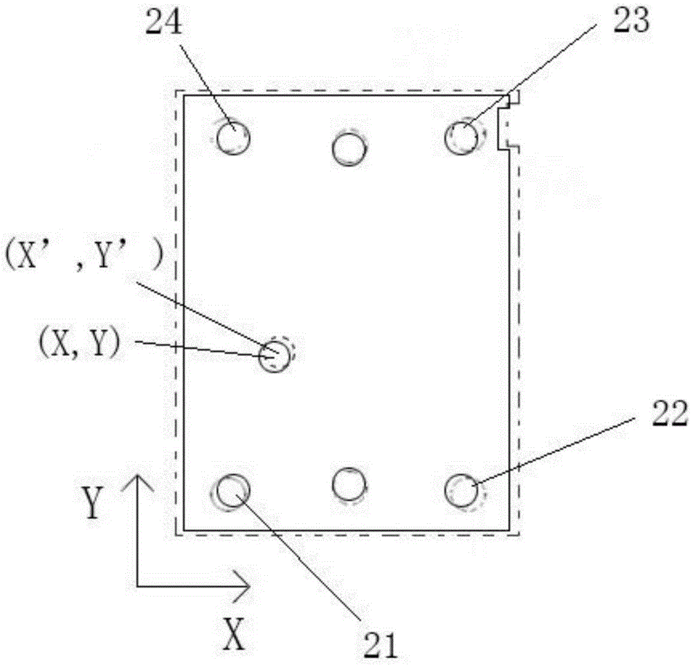
[0052] S4: obtain the position of the positioning target hole 2 of the circuit board after processing, such as image 3 shown;

[0053] S5: Calibrate the drilling position according to the position of the positioning target hole 2 of the processed circuit board and the initial position of the positioning target hole 2 of the circuit board;

[0054] S6: Drilling holes at the calibrated drilling positions.

[0055] The above-mentioned technical solution is the core technical solution of the present invention. It forms pin holes on the circuit board and fixes the circuit board through the pins, and then drills by obtaining the p...

Embodiment approach

[0057] As a preferred embodiment, the S1 step may include:

[0058] S11: a pad (PAD) corresponding to the prefabricated position of the pin hole 1 and the positioning target hole 2 is set on the circuit board;

[0059] S12: determine the pad position;

[0060] S13: Drill out the pin hole 1 and the positioning target hole 2 at the pad position.

[0061] The above steps S11-S13 can be applied to a single-layer circuit board or a multi-layer circuit board. For a common multi-layer circuit board, pads can be provided on the inner layer of the circuit board, and the pin hole 1 and the positioning target can be calibrated through the pads For the forming position of hole 2, the outer layer is laminated on the inner layer to form a multi-layer circuit board, and the position of the pad is determined by the X-ray target machine, which can accurately locate the drilling position of the pin hole 1 and the target hole 2, and prevent the hole after lamination. Drilling positions for pin...


PUM


Abstract

The invention provides a circuit board hole drilling method and relates to the technical field of circuit board production. Through forming a pin hole in the circuit board, the circuit board is fixed through the pin; position data of a positioning target hole in the same board surface as a prefabricated drilling hole after the circuit board is deformed are acquired; according to the position data of the positioning target hole after the circuit board is deformed and position data of the positioning target hole before the circuit board is deformed, a drilling hole position is calibrated; the drilling hole position is accurately positioned, the device for fixing the pin does not need to be adjusted accurately, the adjustment time is reduced, the operation ratio of the drilling machine is improved, and the production efficiency is improved.

Description

technical field [0001] The invention relates to the technical field of circuit board production, in particular to a circuit board drilling method. Background technique [0002] The TWOPIN technology first emerged in Japan, and has been introduced to my country in recent years. This technology is mainly to solve the traditional drilling calibration method. The ratio of the actual production quantity of a machine and equipment to the possible production quantity) is low. The main steps of TWOPIN technology are first planting pins (PIN) on the circuit board, and then fixing the board, backing plate and cover plate together with the glue machine (these processes do not need to be carried out on the drilling machine), and then the package The glued board is placed in the PIN slot of the drilling rig, press the clamp PIN button and clamp the pin through the clamp PIN slot to complete the fixing of the circuit board. After the circuit board is fixed, drill holes on the circuit boar...

Claims


Application Information

Patent Timeline
Patent Type & Authority Applications(China)
IPC IPC(8): H05K3/00
CPCH05K3/0047H05K2203/0214
Inventor 王汝兵朱兴华陈继权陈显任
Owner PEKING UNIV FOUNDER GRP CO LTD
Why Eureka
Try Eureka