
A new type of chip diode manufacturing process and its special welding mold

A manufacturing process and welding mold technology, applied in the field of new chip diode manufacturing process, can solve the problems of restricting the improvement of product electrical yield and production cost, and achieve the effects of low welding stress, improved utilization rate, and reduced cost

Active Publication Date: 2018-02-13
CHANGZHOU ZHIDE ELECTRONICS CO LTD
View PDF6 Cites 0 Cited by
  • Summary
  • Abstract
  • Description
  • Claims
  • Application Information

AI Technical Summary

Problems solved by technology

The defect of this method is that the upper and lower frames are fixed on the welding mold by means of pin hole positioning
[0003] Products produced by the above process, due to welding stress and chip offset phenomenon, restrict the improvement of electrical yield of such products (the current industry electrical yield is 93%)
[0004] In addition, when the product uses chips of different sizes, the upper and lower frame sizes used are also inconsistent. Therefore, it is necessary to use multi-standard frame stamping dies and welding dies, resulting in an increase in production costs

Method used


Image

  • A new type of chip diode manufacturing process and its special welding mold
  • A new type of chip diode manufacturing process and its special welding mold
  • A new type of chip diode manufacturing process and its special welding mold

Examples


Embodiment 1

[0027] The new chip diode manufacturing process of this embodiment, the steps are as follows:

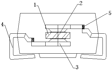
[0028] (1) if figure 1 As shown, the chip 1, the soldering piece 2 and the oxygen-free copper connecting piece 3 are precisely positioned using a special welding mold, so that the P pole connecting piece extends out of the P electrode of the chip horizontally, and the N pole connecting piece extends out of the N electrode of the chip horizontally; Then put the special welding mold in the tunnel furnace and weld at 360°C for 7 minutes. After the welding piece is melted, the P pole connecting piece, the N pole connecting piece and the chip form a stable Z-shaped structure;

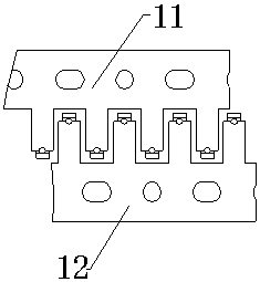
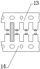
[0029] (2) The chip 1 welded with the connecting piece 3 is taken out by an intelligent manipulator and placed on the laser welding tool; then the frame 4 with several lead brackets distributed inside is placed on the corresponding laser welding tool; image 3 As shown, the lead end of the upper frame 11 is provi...

Embodiment 2

[0032] The new chip diode manufacturing process of this embodiment, the steps are as follows:

[0033] (1) if figure 1 As shown, the chip 1, the soldering piece 2 and the oxygen-free copper connecting piece 3 are precisely positioned using a special welding mold, so that the P pole connecting piece extends out of the P electrode of the chip horizontally, and the N pole connecting piece extends out of the N electrode of the chip horizontally; Then put the special welding mold in the tunnel furnace and weld at 375°C for 12 minutes. After the welding piece is melted, the P pole connecting piece, the N pole connecting piece and the chip form a stable Z-shaped structure;

[0034] (2) Take out the chip 1 welded with the connecting piece 3 through the intelligent manipulator, and place it on the laser welding tool; then place the frame 4 with several lead brackets distributed on the inside on the corresponding laser welding tool; image 3 As shown, the lead end of the upper frame 11...

Embodiment 3

[0037] The new chip diode manufacturing process of this embodiment, the steps are as follows:

[0038] (1) if figure 1 As shown, the chip 1, the soldering piece 2 and the oxygen-free copper connecting piece 3 are precisely positioned using a special welding mold, so that the P pole connecting piece extends out of the P electrode of the chip horizontally, and the N pole connecting piece extends out of the N electrode of the chip horizontally; Then put the special welding mold in the tunnel furnace and weld at 370°C for 10 minutes. After the welding piece is melted, the P pole connecting piece, the N pole connecting piece and the chip form a stable Z-shaped structure;

[0039] (2) Take out the chip 1 welded with the connecting piece 3 through the intelligent manipulator, and place it on the laser welding tool; then place the frame 4 with several lead brackets distributed on the inside on the corresponding laser welding tool; image 3 As shown, the lead end of the upper frame 11...


PUM


Abstract

The invention relates to a novel surface mount diode manufacturing process. The process comprises the steps of accurately positioning a chip, a soldering lug and connecting pieces to weld the chip, the soldering lug and the connecting pieces by a special welding mold, forming a stable z-shaped structure by the chip and the connecting pieces, conducting the laser welding on the overlapped part of the outer end of a downward bending section of an upper frame and the outer end of the connecting piece of a P electrode to fix the overlapped part, and conducting the laser welding on the overlapped part of the outer end of an upward bending section of a lower frame and the outer end of the connecting piece of an N electrode to fix the overlapped part. The special welding mold for implementing the novel surface mount diode manufacturing process comprises a mold body. The mold body is provided with a plurality of welding cavities. The welding cavities are composed of a main cavity, first accessory cavities and second accessory cavities, wherein the first accessory cavities and the second accessory cavities are on the two sides of the main cavity and are respectively in direct communication with the main cavity. According to the technical scheme of the invention, one part of the upper frame and one part of the lower frame of a surface mount diode are replaced by the connecting pieces. Meanwhile, the chip, the soldering lug and the connecting pieces are accurately positioned by the special welding mold. Therefore, the chip offset phenomenon is solved.

Description

technical field [0001] The invention relates to a novel chip diode manufacturing process, and also relates to a special welding mold for realizing the new chip diode manufacturing process. Background technique [0002] At present, the chip diode series products on the market adopt the method of directly placing the chip, soldering piece, upper frame and lower frame in the welding mold, and then placing the welding mold in the welding furnace for soldering. The defect of this method is that the upper and lower frames are fixed on the welding mold by means of pin hole positioning. During the welding process, the frame will expand when heated, and the thermal expansion coefficient of the frame is different from that of the chip, which will generate welding stress on the chip, and there will be a phenomenon of chip offset, resulting in problems such as poor welding and excessive welding stress, which will affect the electrical yield of the product. And reliable performance, res...

Claims


Application Information

Patent Timeline
Patent Type & Authority Patents(China)
IPC IPC(8): H01L33/48H01L33/62H01L21/68H01L21/60
CPCH01L21/68H01L24/84H01L33/486H01L33/62H01L2224/84136H01L2933/0066H01L2224/32245H01L2224/33H01L2224/33181H01L2924/181H01L2924/00012
Inventor 刘新华
Owner CHANGZHOU ZHIDE ELECTRONICS CO LTD
Learn More