A method for coating LED fluorescent powder glue

A phosphor and LED module technology, applied in the direction of semiconductor devices, electrical components, circuits, etc., can solve the problems of difficult to obtain the ideal phosphor powder shape, complex phosphor coating methods, etc., to improve the consistency of light color and cost Low, easy-to-operate effect

Active Publication Date: 2017-11-17
HUAZHONG UNIV OF SCI & TECH
View PDF5 Cites 0 Cited by
  • Summary
  • Abstract
  • Description
  • Claims
  • Application Information

AI Technical Summary

Problems solved by technology

[0007] Aiming at the above defects or improvement needs of the prior art, the present invention provides a phosphor glue coating method, the purpose of which is to realize that the thickness of the middle phosphor layer is greater than that of the phosphors on both sides by dispensing glue on the upper surface of the chip and the side of the chip respectively. The thickness of the phosphor powder gel shape, so as to obtain better spatial color uniformity, thus solving the technical problem that the current phosphor powder coating method is complicated and it is difficult to obtain the ideal phosphor powder gel shape

Method used


Image

  • A method for coating LED fluorescent powder glue
  • A method for coating LED fluorescent powder glue
  • A method for coating LED fluorescent powder glue

Examples


Embodiment 1

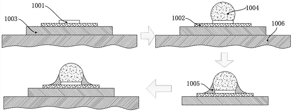
[0042] S1: Place the LED module that has completed the chip mounting and circuit connection on the heating plate. The LED chip is a rectangular chip, the thickness of the rectangular chip is 1 mm, and the length L and width W of the rectangular chip are both 3 mm. The ratio of the volume of phosphor glue coated on the upper surface of the chip to the area of ​​the upper surface of the rectangular chip is (L+W) / 8, and the heating temperature of the LED module is 100°C.

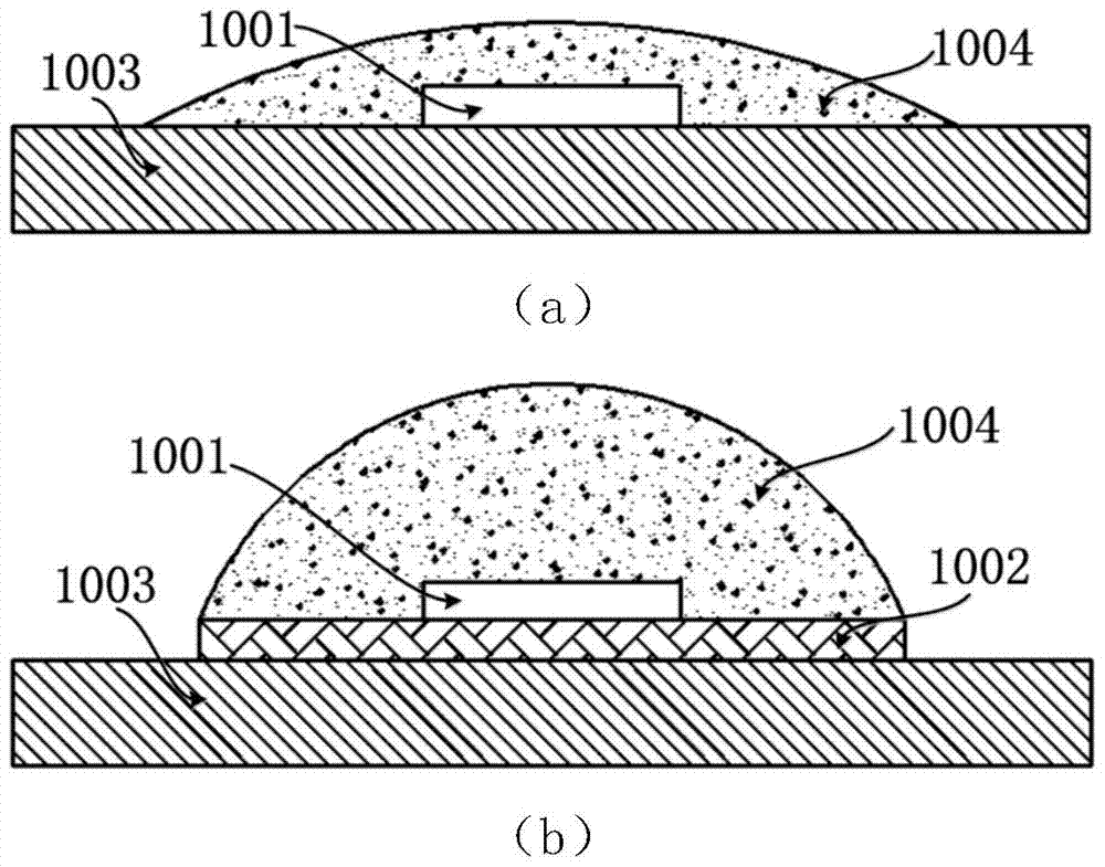
[0043] S2: After the temperature of the LED module is stabilized at 100°C, apply 6.75 microliters of fluorescent powder glue with a set concentration of 0.02 g / ml on the upper surface of the chip, and stand still for a certain period of time until the set amount of phosphor powder is applied The glue forms a spherical-segment-like topography on the upper surface of the chip.

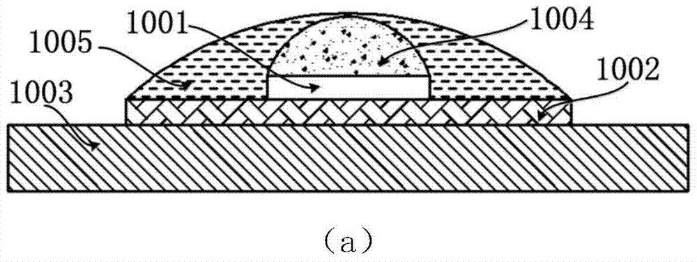
[0044] S3: Remove the LED module from the heating substrate, and apply 4.1 microliters of fluorescent powder glue with a set concentrati...

Embodiment 2

[0047] S1: Place the LED module that has completed the chip mounting and circuit connection on the heating plate. The LED chip is a rectangular chip, the thickness of the rectangular chip is 0.1 mm, and the length L and width W of the rectangular chip are both 1 mm. The ratio of the coating volume to the area of ​​the upper surface of the rectangular chip was (L+W) / 2, and the heating temperature of the LED module was 150°C.

[0048] S2: After the temperature of the LED module is stabilized at 150°C, apply 1 microliter of fluorescent powder glue with a set amount of 1 g / ml on the upper surface of the chip, and stand still for a certain period of time until the set amount of phosphor powder is applied. The glue forms a spherical-segment-like topography on the upper surface of the chip.

[0049] S3: Remove the LED module from the heating substrate, and apply 0.8 microliters of phosphor glue with a set concentration of 1 g / ml on the side surface of the chip, and the concentration ...

Embodiment 3

[0052] S1: Place the LED module that has completed the chip mounting and circuit connection on the heating plate. The LED chip is a rectangular chip, the thickness of the rectangular chip is 0.01 mm, and the length L and width W of the rectangular chip are both 0.5 mm. The ratio of the coating volume to the area of ​​the upper surface of the rectangular chip was 3(L+W) / 2, and the heating temperature of the LED module was 180°C.

[0053] S2: After the temperature of the LED module is stabilized at 180°C, apply 0.375 microliters of fluorescent powder glue with a set concentration of 4 g / ml on the upper surface of the chip, and stand still for a certain period of time until the set amount of phosphor powder is applied The glue forms a spherical-segment-like topography on the upper surface of the chip.

[0054] S3: Remove the LED module from the heating substrate, and apply 0.2 microliters of fluorescent powder glue with a set concentration of 5 g / ml on the side surface of the chi...


PUM


Abstract

The invention discloses an LED fluorescent powder glue coating method, and belongs to the field of LED packaging. The method comprises the following steps: S1, placing an LED module with completed chip mounting and circuit connection on a heating plate with a temperature of 100 to 180 DEG C; S2, after the temperature of the LED module is stable, coating the upper surface of a chip with a set amount of fluorescent powder glue, and leaving it alone for certain time until the set amount of fluorescent powder glue forms a partially spherical morphology on the upper surface of the chip; S3, taking the LED module from the heating substrate, and coating the side surface of the chip with a set amount of fluorescent powder glue; and S4, after the morphology of the fluorescent powder glue is stable, executing a solidification process to obtain a predetermined fluorescent powder glue morphology. The method provided by the invention is simple to operate and low in cost, can flexibly control the fluorescent powder glue morphology, obtains the fluorescent powder glue morphology in which the thickens of an intermediate fluorescent powder layer is greater than the thicknesses of fluorescent powder layers at two sides, is low in packaging cost and can be applied to industries for LED packaging in a large scale.

Description

technical field [0001] The invention belongs to the field of LED packaging, and more specifically relates to a method for coating LED fluorescent powder glue. Background technique [0002] LED (Light Emitting Diode) is a semiconductor light-emitting device based on the principle of P-N junction electroluminescence. It has the advantages of high electro-optical conversion efficiency, long service life, environmental protection and energy saving, and small size. It is known as the green lighting source in the 21st century. Due to the unique advantages of LED, it has been widely used in many fields, and is considered by the industry to be the main development direction of lighting technology in the future, with huge market potential. Among them, white LED products are the most widely used. [0003] High-power white LEDs are usually mixed with two wavelengths of blue light and yellow light or three-wavelength light of blue light, green light and red light. Due to the simple pr...

Claims


Application Information

Patent Timeline
Patent Type & Authority Patents(China)
IPC IPC(8): H01L33/50H01L33/00
CPCH01L33/50H01L33/502H01L33/505H01L2933/0041
Inventor 罗小兵余兴建刘发龙舒伟程谢斌马预谱
Owner HUAZHONG UNIV OF SCI & TECH
Why Eureka
Try Eureka