

Non-organic-glue wafer-level package method and LED flip chip package body
A wafer-level packaging, flip-chip technology, applied in semiconductor devices, electrical components, circuits, etc., can solve the problems of high bonding processing temperature, damage to flip-chip, etc., to achieve high light transmittance, long life, Avoid low-yield effects
- Summary
- Abstract
- Description
- Claims
- Application Information
AI Technical Summary
Problems solved by technology
Method used
Image

Examples
Embodiment 1
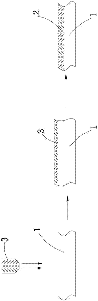
[0039] The invention provides a method for wafer-level packaging free of organic glue, the method comprising the following steps,
[0040] S1. Prepare flat silicate glass and LED flip-chip wafers. The LED flip-chip wafers have been formed on the epitaxial layer of the wafer through chip technology to form electrodes and other processes, but have not been pre-cracked and processed. sliced wafers;
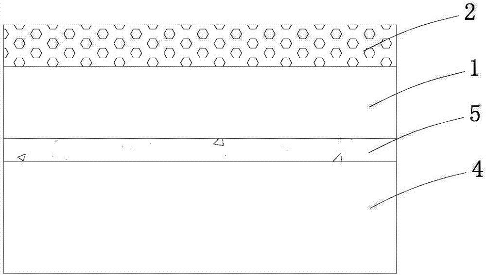
[0041] S2. Form a phosphor layer on one surface of the glass, and use the other surface corresponding to the surface as the surface to be bonded;
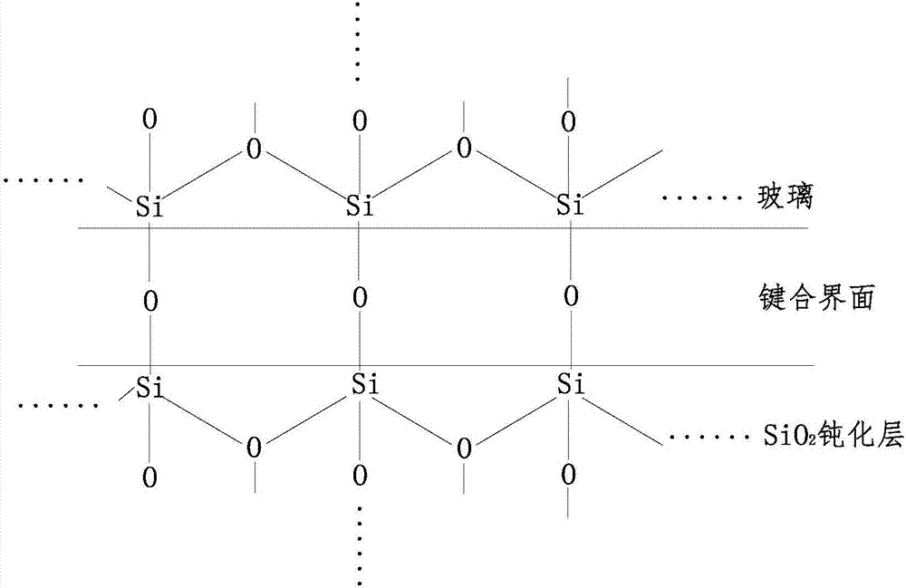
[0042] S3, forming a SiO2 passivation layer on the light-emitting surface of the LED flip-chip wafer;
[0043] S4, directly bonding the surface to be bonded of the glass after step S2 to the passivation layer, so that the glass is directly fixed to the light-emitting surface of the LED flip-chip wafer;
[0044] S5. Cutting, cutting the glass-fixed LED flip-chip wafer after step S4 into LED flip-chip packages of corresponding sizes.
...
example 1
[0065] 1. Use acetone as a carrier to evenly spray yellow and red phosphors on the surface of a 5-inch soda-lime silicate glass substrate, heat to a softening temperature of 700°C-720°C, and keep warm for 5 minutes.
[0066] 2. Use magnetron sputtering to form a 1 μm thick SiO2 passivation layer on the light-emitting surface of a 4-inch non-pre-cracked LED flip-chip wafer.
[0067] 3. Plasma cleaning or ultrasonic cleaning of the flip chip and the soda lime silicate glass to be bonded for 5 minutes, followed by rinsing with deionized water for 1-5 minutes.
[0068] 4. Prepare H with a volume ratio of 4:1 2 SO 4 and H 2 o 2 solution, where H 2 SO 4 and H 2 o 2 The mass percent concentration of the solution is 98% and 30%, the solution temperature is 110° C., and the cleaning time is 15 minutes. The materials to be bonded are cleaned twice, and then cleaned with deionized water for 5 minutes.
[0069] 5. Prepare a certain volume ratio of activation solution NH 3 ·H 2 O...
example 2
[0073] 1. Use tetrahydrofuran as a carrier to evenly spray yellow powder and red powder on the surface of a 7-inch borosilicate glass substrate, heat to a softening temperature of 800-900°C, and keep warm for 10 minutes.
[0074] 2. Use MOCVD (chemical vapor deposition) to form a layer of 1 μm thick SiO2 passivation layer on the light-emitting surface of a 6-inch non-pre-cracked LED flip-chip wafer.
[0075] 3. Plasma cleaning or ultrasonic cleaning flip chip and borosilicate glass to be bonded for 5 minutes, rinse with deionized water for 1-5 minutes.
[0076] 4. Put the glass and the LED flip-chip wafer into the plasma processor, use O2 plasma to bombard the passivation layer of the LED flip-chip wafer to be bonded and the surface to be bonded of the borosilicate glass, (plasma Parameter setting of the processing instrument: the vacuum degree of the vacuum chamber is evacuated to 0.1Pa, oxygen is introduced, the processing pressure is 20Pa, 5 minutes, and the processing powe...
PUM
 Abstract
Description
Claims
Application Information