A process method and refining equipment system for a refined light conversion body to fit and package an LED

A process method and LED package technology, applied in the direction of semiconductor devices, electrical components, circuits, etc., can solve the problems of product consistency, low production efficiency of packaged LEDs, and the influence of thermal overstress, so as to improve production efficiency and optimize The product rate, the removal of the external bonding layer process, and the effect of improving the consistency of light and color

Active Publication Date: 2017-12-22
JIANGSU CHERRITY OPTRONICS CO LTD
View PDF8 Cites 0 Cited by
  • Summary
  • Abstract
  • Description
  • Claims
  • Application Information

AI Technical Summary

Problems solved by technology

Although this method improves the uniformity of the coating thickness of the light conversion body through the screen printing process, and improves the uniformity of the phosphor particle distribution, so as to achieve the purpose of improving the yield; but there are still the following obvious deficiencies: one is that the screen printing The light converter of silicone resin is coated on the surface of the LED chip, and then due to the influence of thermal overstress during the baking and curing process, it will still cause local bubbles to form on the coating surface of the light converter coating and the LED chip to form unevenness The second is to fill the sealing mold or the lens cover with silica gel and package the LED chip coated with the light conversion body, and then the overall structure is baked and cured due to the influence of thermal overstress, which will still cause cracks in the sealing mold or lens cover. Bubbles are generated locally on the silicone surface layer to form uneven defects
The purpose of this method is to provide light converters uniformly arranged around the LED to prevent damage, so as to obtain an LED covered with a light converter layer and an LED device with the LED covered with a light converter layer; but there are also the following obvious Disadvantages: First, during the curing process of the fluorescent resin composition of the light conversion body, due to the influence of thermal overstress, it will still cause local bubbles to form on the surface layer of the light conversion body to form uneven defects; LEDs will still be affected by thermal overstress, resulting in a decrease in light efficiency during use of the LED; third, the process in the entire packaging process is relatively cumbersome, and the production efficiency of the packaged LED is not high; The displacement of the chip will inevitably lead to a decrease in the yield rate
Although the object of the invention of this proposal is to improve the uniformity of color and brightness, ease of manufacture, degree of freedom in design, etc. of the semiconductor light-emitting element to which the phosphor-containing resin layer is attached by the resin sheet laminate, but There are also the following obvious deficiencies: one is that the phosphor resin sheet used is a cured phosphor resin sheet, which will not be able to effectively eliminate possible residual pores, unevenness or other processing defects; the other is that in the bonding process, Pressing the pressure tool from the side of the semiconductor light-emitting element will damage the semiconductor light-emitting element; the third is to use the adhesive bonding process in the phosphor resin layer, which is difficult to remove the residue in the bonded semiconductor light-emitting element. The bonding process is very easy to produce air holes, which will reduce the yield rate. At the same time, the existence of the bonding layer also reduces the light extraction efficiency of the LED element; the fourth is the phosphor resin sheet bonded to the light-emitting surface of the semiconductor light-emitting element. If the base material is not peeled off, it will directly affect the light effect of the semiconductor light-emitting element; fifth, the phosphor resin layer is presented in the form of multiple blocks arranged in rows repeatedly in the length direction, but to realize the multiple regions of the phosphor resin layer Block configuration, the actual operation procedure is cumbersome, which will affect the packaging efficiency of the entire component, and the positional layout error of multiple blocks will directly affect the accuracy of the subsequent bonding with the light-emitting element, and between multiple blocks. If the size and thickness cannot meet the consistency requirements, it may lead to serious product consistency problems

Method used


Image

  • A process method and refining equipment system for a refined light conversion body to fit and package an LED
  • A process method and refining equipment system for a refined light conversion body to fit and package an LED
  • A process method and refining equipment system for a refined light conversion body to fit and package an LED

Examples


Embodiment 1

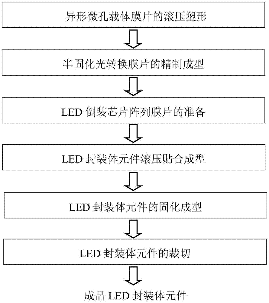
[0063] Example 1. see figure 1 , figure 2 and Figure 6 As shown, the present invention proposes a process for bonding and packaging LEDs with a refined light conversion body, which includes rolling molding of special-shaped microporous carrier membranes, refined molding of semi-cured light conversion membranes, and LED flip-chip array membranes. The preparation of the sheet, the rolling and bonding of the LED package components, the curing and molding of the LED package components and the cutting process of the LED package components are a flow-type continuous process. The specific steps include the following:

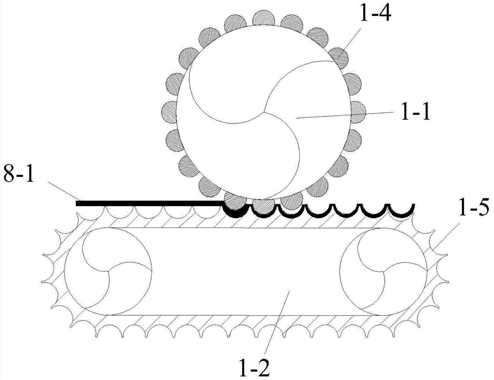
[0064] Step 1, rolling shaping of the special-shaped microporous carrier membrane: the microporous carrier membrane is passed through the first rolling device with a bump array and the second rolling device with a groove array that are aligned to each other. Rolling and molding to obtain a special-shaped microporous carrier membrane with a groove array; wherein: t...

Embodiment 2

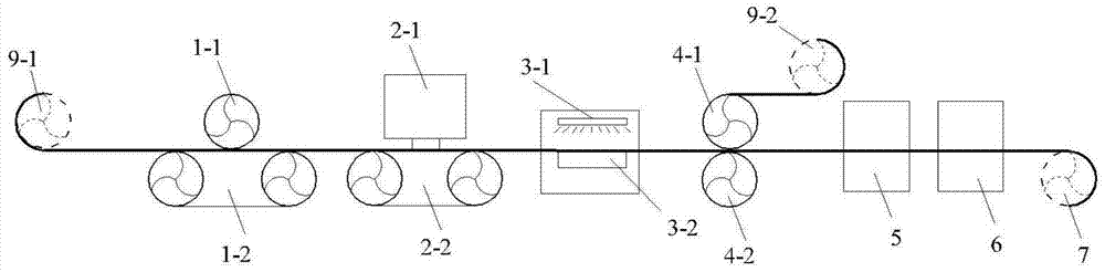
[0096] Embodiment 2: The refining equipment system adopted in the process method of a refined light conversion body packaged LED proposed by the present invention, which includes a special-shaped microporous carrier film roll for shaping the special-shaped microporous carrier film Compression molding device, semi-cured light conversion film precision molding device for forming a pre-cured light conversion film on the shaped special-shaped microporous carrier film, and a rolling press for rolling and laminating molding of LED package components Laminating device; the special-shaped microporous carrier film rolling forming device, semi-cured light conversion film fine forming device and rolling laminating device are arranged in sequence to form a coordinated linkage process equipment; wherein:

[0097] The special-shaped microporous carrier membrane rolling molding device includes a first rolling device with a bump array and a second rolling device with a groove array arranged in...


PUM


Abstract

The invention relates to a refining light conversion body fitting packaging LED process method and refining equipment system. The process method comprises the continuous flow process formed by rolling molding of a special-shaped micropore carrier film, refining molding of a semi-curing light conversion film, preparation of an LED flip chip array film, rolling and fitting molding of LED packaging body elements, curing molding of the LED packaging body elements and the cutting process of the LED packaging body elements. The method has the substantial advantage of the refining light conversion body, and especially the method can meet the requirements of the continuous flow process of the organic silicon resin light conversion body fitting packaging LED so that the production efficiency and the superior product rate of industrial batch LED packaging can be enhanced.

Description

technical field [0001] The invention belongs to the technical field of light conversion body packaging LEDs, and in particular relates to a process method and a refining equipment system for bonding and packaging LEDs with a refined organic silicon resin light conversion body. Background technique [0002] LED has the advantages of high brightness, low heat, long life, environmental protection, renewable utilization, etc., and is called the most promising new generation of green lighting source in the 21st century. At present, although the theoretical life of LEDs can reach more than 100,000 hours, in actual use, due to the constraints of various factors such as chip failure, packaging failure, thermal overstress failure, electrical overstress failure or / and assembly failure, among them Package failure is particularly prominent, which makes LEDs prematurely experience light decay or light failure, which will hinder the progress of LEDs as a new type of energy-saving lighting...

Claims


Application Information

Patent Timeline
Patent Type & Authority Patents(China)
IPC IPC(8): H01L33/50
CPCH01L33/501H01L33/507H01L2933/0041
Inventor 何锦华
Owner JIANGSU CHERRITY OPTRONICS CO LTD
Why Eureka
Try Eureka