Touch substrate, manufacturing method and display device
A technology for display devices and substrates, applied in optics, instruments, electrical digital data processing, etc., can solve problems affecting touch sensing accuracy, assembly tolerances, etc.
- Summary
- Abstract
- Description
- Claims
- Application Information
AI Technical Summary
Problems solved by technology
Method used
Image

Examples
Embodiment Construction
[0037] Embodiments of the present invention will be described in detail below with reference to the accompanying drawings.
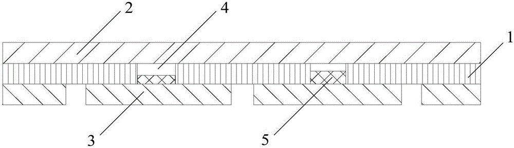
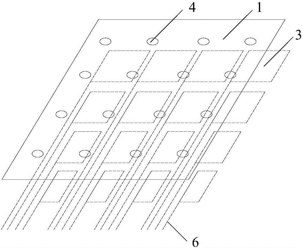
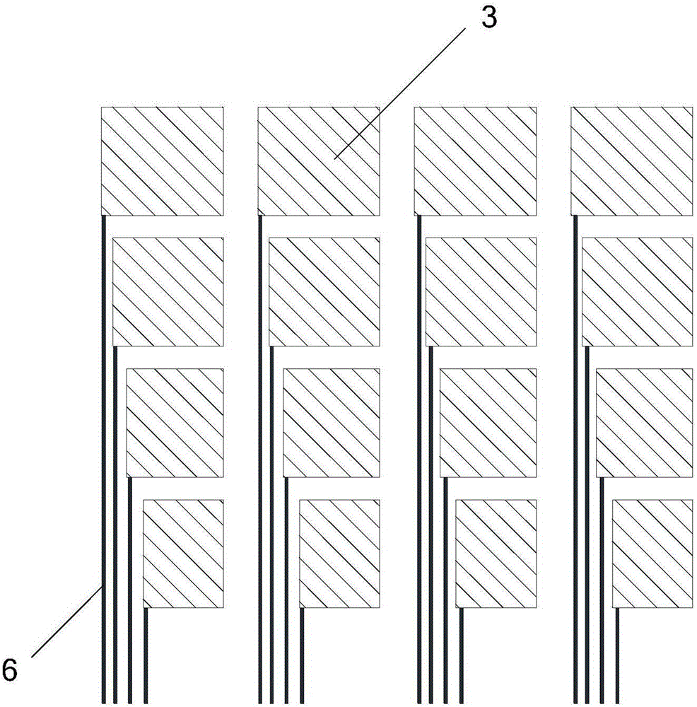
[0038] An embodiment of the present invention provides a touch substrate, such as figure 1 , figure 2 As shown, the touch control substrate includes a substrate 1 provided with several through holes 4; on the first surface (upper surface) of the substrate 1, a first electrode 2 covering several through holes 4 is formed (not in the figure 2 shown in ); on the second surface (lower surface) of the substrate 1 opposite to the first surface, a plurality of second electrodes 3 each corresponding to a touch area are formed; the second electrodes 3 are at least partially in at least one place Surrounding the edge of the through hole 4; the through hole 4 is provided with an elastic conductor block 5 for forming an electrical connection between the first electrode 2 and the second electrode 3 at both ends of the through hole 4 when the substrate 1 is pressed...
PUM
 Abstract
Description
Claims
Application Information
 - R&D Engineer
- R&D Manager
- IP Professional
- Industry Leading Data Capabilities
- Powerful AI technology
- Patent DNA Extraction
Browse by: Latest US Patents, China's latest patents, Technical Efficacy Thesaurus, Application Domain, Technology Topic.
© 2024 PatSnap. All rights reserved.Legal|Privacy policy|Modern Slavery Act Transparency Statement|Sitemap