Copper interconnection structure, manufacturing method thereof, and electronic device

A technology of copper interconnect structure and manufacturing method, which is applied in semiconductor/solid-state device manufacturing, circuits, electrical components, etc., can solve the problems of dish-shaped defects in metal areas, erosion of copper metal, and erosion of dielectric areas, and achieves less damage and reduction. The effect of height change

Active Publication Date: 2018-11-16
SEMICON MFG INT (SHANGHAI) CORP
View PDF4 Cites 0 Cited by
  • Summary
  • Abstract
  • Description
  • Claims
  • Application Information

AI Technical Summary

Problems solved by technology

CMP may also cause dishing defects in metal regions and erosion in dielectric regions
In addition, chemicals such as abrasive fluids that have not been cleaned near the metal / media interface may attack the copper metal

Method used


Image

  • Copper interconnection structure, manufacturing method thereof, and electronic device
  • Copper interconnection structure, manufacturing method thereof, and electronic device
  • Copper interconnection structure, manufacturing method thereof, and electronic device

Examples


Embodiment 1

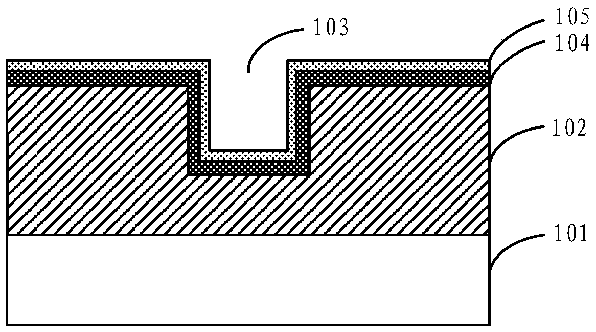
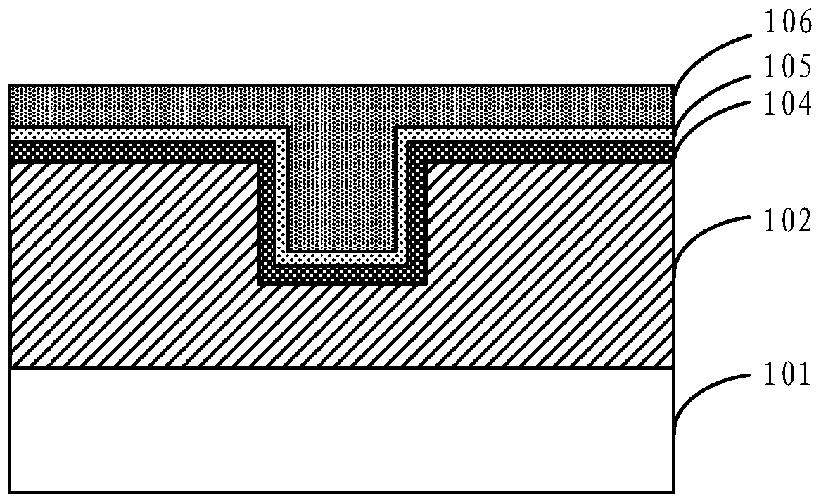
[0027] Below, refer to Figure 2a-Figure 2e with image 3 The detailed steps of the manufacturing method of the copper interconnection structure proposed by the present invention will be described. Figure 2a-2e A schematic cross-sectional view of a semiconductor device obtained in key steps of a method for manufacturing a copper interconnection structure according to an embodiment of the present invention is shown.

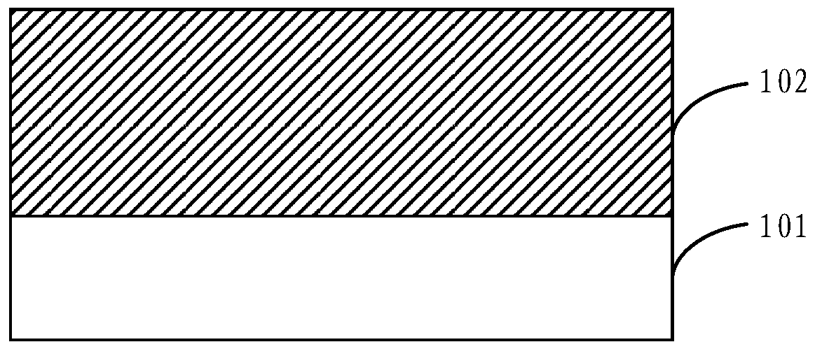
[0028] First, refer to Figure 2a , in step a), a semiconductor substrate 201 is provided. The constituent material of the semiconductor substrate 201 may be undoped single crystal silicon, single crystal silicon doped with impurities, silicon-on-insulator (SOI) or the like. Isolation trenches, buried layers, various well structures or lower interconnection structures may be formed in the semiconductor substrate 201 , which are omitted in the illustration for simplicity.

[0029] continue to refer Figure 2a , in step b), an interlayer dielectric layer 202 ,...

Embodiment 2

[0044] The present invention also provides a copper interconnection structure, which is manufactured by the method described in the above-mentioned embodiments. According to the copper interconnection structure provided by the present invention, the CMP process is replaced by an etch-back process, which can reduce the height change of the copper interconnection line on the semiconductor product caused by the CMP process, and the damage to the interlayer dielectric layer caused by moisture absorption Also smaller.

Embodiment 3

[0046] The present invention also provides an electronic device, including the copper interconnection structure described in the second embodiment. Wherein, the copper interconnection structure is the copper interconnection structure described in the second embodiment, or the copper interconnection structure obtained according to the manufacturing method described in the first embodiment.

[0047] The electronic device of this embodiment can be any electronic product or equipment such as mobile phone, tablet computer, notebook computer, netbook, game console, TV set, VCD, DVD, navigator, camera, video recorder, voice recorder, MP3, MP4, PSP, etc. , can also be any intermediate product including the copper interconnection structure. The electronic device of the embodiment of the present invention has better performance due to the above-mentioned copper interconnection structure.


PUM


Abstract

The invention provides a copper interconnecting device, a manufacturing method thereof and an electronic device. The method comprises the following steps: (a) providing a semiconductor substrate; (b) forming an interlayer dielectric layer, an etching barrier layer and a mask film layer on the semiconductor substrate in sequence; (c) etching the mask film layer, the etching barrier layer and the interlayer dielectric layer so as to form a groove in the interlayer dielectric layer; (d) depositing flowable copper layers in the groove and on the mask film layer; and (e) etching back the flowable copper layers so as to form a copper interconnecting line. According to the manufacturing method of the copper interconnecting structure provided by the invention, a CMP technology is replaced by adopting an etching-back technology, so that the height change of the copper interconnecting line on a semiconductor product caused by the CMP technology can be reduced, and the damage for the interlayer dielectric layer caused by moisture absorption is also little.

Description

technical field [0001] The invention relates to the technical field of semiconductors, in particular to a copper interconnection structure, a manufacturing method thereof, and an electronic device. Background technique [0002] In a semiconductor integrated circuit, signal transmission between semiconductor devices requires high-density metal interconnection lines. The traditional metal interconnection is made of aluminum metal, but with the continuous shrinking of the device feature size in the integrated circuit chip, the current density in the metal wiring continues to increase, and the response time continues to shorten. The traditional aluminum interconnection line has reached Craft limit. When the process size is smaller than 130nm, the traditional aluminum interconnection technology has been gradually replaced by copper interconnection technology. Compared with aluminum metal, copper metal has lower resistivity and longer electromigration life. Using copper technolo...

Claims


Application Information

Patent Timeline
Patent Type & Authority Patents(China)
IPC IPC(8): H01L21/768H01L23/52
Inventor 张海洋张城龙
Owner SEMICON MFG INT (SHANGHAI) CORP
Why Eureka
Try Eureka