Tin alloy electroplating solution for solder bumps including perfluoroalkyl surfactant

a technology of perfluoroalkyl surfactant and tin alloy, which is applied in the direction of semiconductor devices, semiconductor/solid-state device details, electrical apparatus, etc., can solve the problems of reducing the size of the system or improving the electrical performance, defectiveness, yield and quality of products, and formation of empty spaces inside bumps, so as to improve the surface tension, wettability and spreadability of tin-based electroplating solution, and improve the current efficiency of the plating

Active Publication Date: 2018-01-16
APCT
View PDF3 Cites 0 Cited by
  • Summary
  • Abstract
  • Description
  • Claims
  • Application Information

AI Technical Summary

Benefits of technology

[0007]An object of the present invention is to provide a perfluoroalkyl surfactant-containing tin-based electroplating solution for the formation of tin-based solder bumps on a metal-based UBM layer for a flip chip package by electroplating that is advantageous in terms of current efficiency, leaves no cracks in intermetallic compound (IMC) layers and no empty spaces inside bumps, can be used to form bumps with high flatness and small height variation, and is applicable to high speed plating. A further object of the present invention is to provide a method of forming solder bumps for a flip chip by using the tin-based electroplating solution.
[0017]After the formation of metal pillars on an UBM layer, solder bumps can be formed on the metal pillars using the tin-based electroplating solution of the present invention. The presence of the fluorinated surfactant can improve the surface tension, wettability, and spreadability of the tin-based electroplating solution. As a result, the current efficiency of the plating process can be enhanced, the occurrence of cracks in intermetallic compound layers and the formation of empty spaces inside bumps can be prevented, height variations of WID and WIW bumps can be reduced, and a flip chip package can be obtained whose plating film properties are excellent even in the high speed plating range (10 to 19 A / dm2).

Problems solved by technology

However, these conventional processes have limitations in achieving reduced system size or improved electrical performance.
For example, there are problems associated with defectiveness, yield, and quality of products, such as height variations of within die (WID) and within wafer (WIW) bumps, the formation of empty space inside bumps, and the occurrence of cracks in intermetallic compound layers.

Method used


Image

  • Tin alloy electroplating solution for solder bumps including perfluoroalkyl surfactant
  • Tin alloy electroplating solution for solder bumps including perfluoroalkyl surfactant
  • Tin alloy electroplating solution for solder bumps including perfluoroalkyl surfactant

Examples


example 1

on of Tin-Silver Plating Solution

[0062]Tin methanesulfonate (based on the final tin content (95 g / L)), silver methanesulfonate (based on the final silver content (2.0 g / L)), 100 g / L of methanesulfonic acid, 0.1 mg / L of potassium perfluorinated octyl sulfonate, 13.5 g / L of polyoxyethylenestyrenic phenyl ether, 1.5 g / L of polyoxyethylene bisphenol F ether, and 270 g / L of thiodiglycol as a complexing agent were mixed with stirring and filtered through a cartridge filter having a pore size of several micrometers to prepare a tin-silver alloy plating solution.

example 2

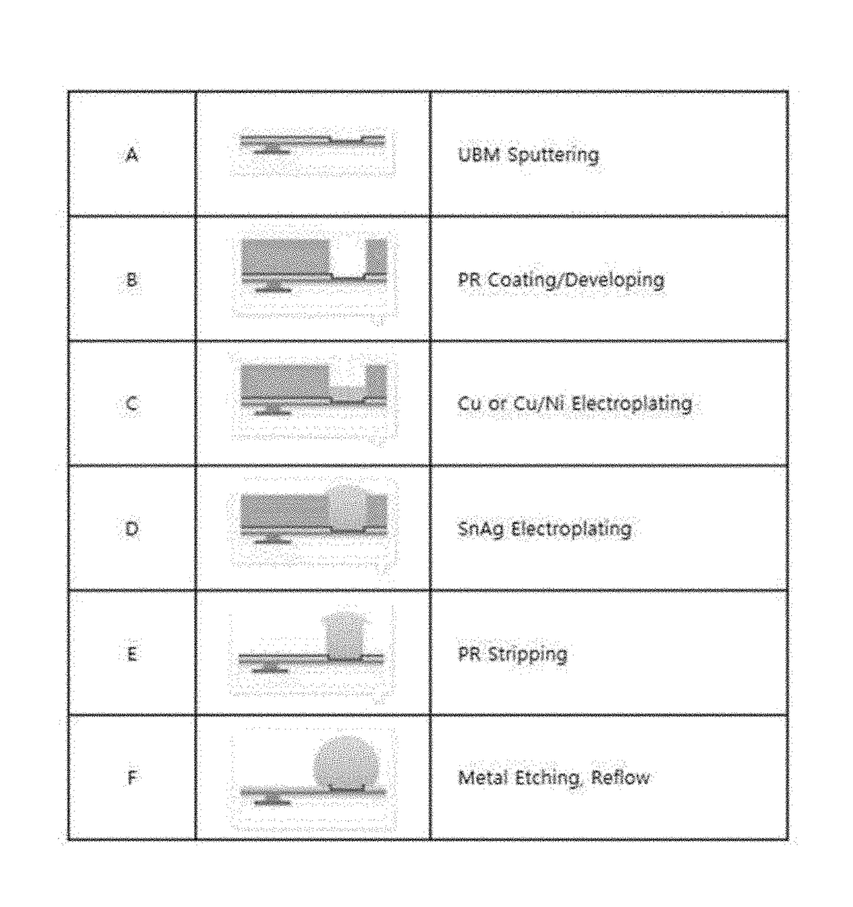
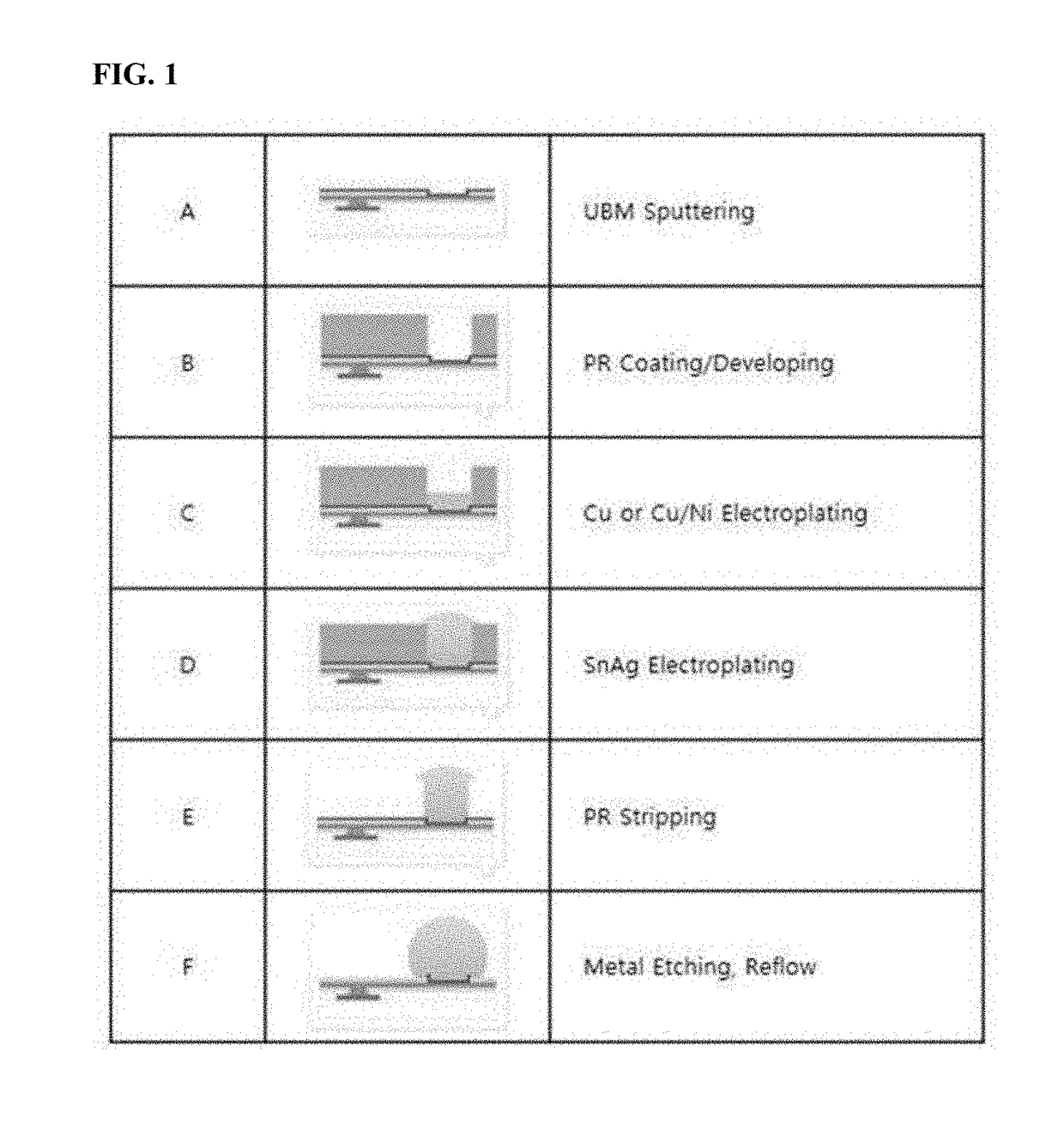
istics of Tin-Based Solder Bumps

[0064]In this example, the shapes and characteristics of tin-silver alloy bumps were observed. The tin-silver electroplating solution of Example 1 was electroplated on the copper pillars, which were formed on the 12-inch patterned wafer in Preparative Example 1, to form solder bumps. The tin-silver electroplating was performed at a current density of 13 A / dm2 while stirring the plating solution at room temperature. The plating speed was 6.6 μm / min at 13 A / dm2. A current efficiency of 99.5% and a silver content of 2.2% were attained. After heating to 240° C. at a rate of 2° C. / min and cooling at a rate of 3° C. / min, solder reflow was performed. The solder bumps were well patterned (bump CD 20-60 μm, bump pitch 95-190 μm) and the plating tendency was good regardless of the shape (pillar or mushroom shape) of the solder bumps. Meanwhile, tin-silver plating was performed at different current densities. The current efficiencies of the plating were found to...

example 3

of the Fluorinated Surfactant

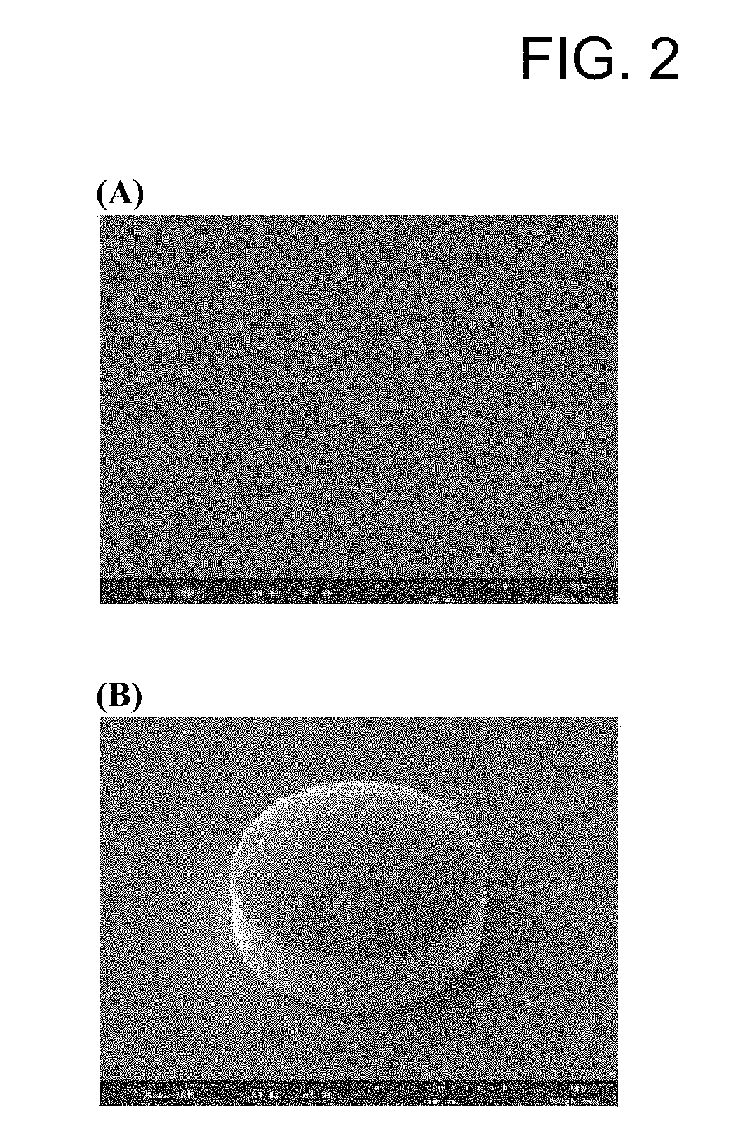
[0066]In this example, the shape and characteristics of tin-silver alloy bumps were observed. Similarly to Evaluation Example 1, the tin-silver electroplating solution of Example 1 was electroplated on the 12-inch patterned wafer formed with the under bump metallurgy layer, which was prepared in Preparative Example 1, to form solder bumps. Example 3 was different from Evaluation Example 1 in that the plated patterned wafer used in Preparative Example 1 was cut into a test piece having a size of 3×3 cm2, which was used as a cathode, a platinum-coated titanium electrode was used as an anode, and galvanostatic plating was performed at current densities of 5 and 10 A / dm2 while stirring 250 mL of the electroplating solution at a rate of 250 rpm until the thickness reached 20 μm. The characteristics of the solder bumps were measured and the results are shown in Table 2 and FIGS. 5 (5a) and 6 (6a).


PUM

PropertyMeasurementUnit
concentrationaaaaaaaaaa
particle sizeaaaaaaaaaa

Abstract

Disclosed is a tin-based electroplating solution for forming solder bumps of a flip chip package. The tin-based electroplating solution includes tin methanesulfonate, silver methanesulfonate, methanesulfonic acid, a fluorinated surfactant, an aromatic polyoxyalkylene ether, and water. Also disclosed is a method for forming solder bumps by using the electroplating solution. The method includes (1) electroplating a silicon wafer having a protective layer through which an electrode pad is exposed and an under bump metallurgy (UBM) layer with a copper or copper / nickel plating solution to form copper or copper / nickel pillars on the under bump metallurgy layer and (2) electroplating the pillars with the tin-based electroplating solution to form solder bumps.

Description

CROSS REFERENCE TO PRIOR APPLICATIONS[0001]This application claims priority to Korean Patent Application No. 10-2014-0098394 filed Jul. 31, 2014, which is hereby incorporated by reference in its entirety.BACKGROUND OF THE INVENTION[0002]1. Field of the Invention[0003]The present disclosure relates to a tin-based electroplating solution that is used to form solder bumps in a flip-chip packaging process.[0004]2. Description of the Related Art[0005]With the advent of small, slim, high-performance electronics, there has been an increasing demand for fast operation and improved electrode density of essential devices, such as memories. Under such circumstances, flip-chip packaging techniques are rapidly extended and applied to the fabrication of electronic devices. Conventional wire bonding processes involve connecting chips to boards with fine wires. Tape automated bonding (TAB) processes involves arranging chips on flexible tapes. However, these conventional processes have limitations i...

Claims


Application Information

Patent Timeline
Patent Type & Authority Patents(United States)
IPC IPC(8): H01L23/00C25D5/10C25D7/12C25D5/02C25D3/46C25D3/32
CPCH01L24/11C25D3/32C25D7/123C25D5/10C25D3/46C25D5/02H01L2924/10253H01L2924/0132H01L2224/94H01L2224/13155H01L2224/13147H01L2224/13111H01L2224/11849H01L2224/11462H01L2224/1147H01L2224/05647H01L2224/0345H01L24/94H01L24/13H01L24/05H01L24/03H01L2924/01047H01L2924/00014H01L2224/11H01L2224/03C25D3/38C25D3/60C25D5/12C25D5/617C25D3/56
Inventor KO, JUNG WOOOH, JEONG HUNPARK, KYU BINPARK, HYUN KOOKJUNG, HEUNG SU
Owner APCT
Why Eureka
Try Eureka