Unlock instant, AI-driven research and patent intelligence for your innovation.
Underfill material and method of manufacturing semiconductor device using same
What is Al technical title?
Al technical title is built by PatSnap Al team. It summarizes the technical point description of the patent document.
An underfill material, semiconductor technology, used in semiconductor/solid-state device manufacturing, semiconductor devices, semiconductor/solid-state device components, etc., can solve problems such as narrow mounting edges, achieve wide mounting edges, achieve no-void mounting, and good solder The effect of engagement
Active Publication Date: 2019-10-22
DEXERIALS CORP
View PDF10 Cites 0 Cited by
Summary
Abstract
Description
Claims
Application Information
AI Technical Summary
This helps you quickly interpret patents by identifying the three key elements:
Problems solved by technology
Method used
Benefits of technology
Problems solved by technology
Also, the underfill material only fits well with generally defined installation curves, the installation edge ( )narrow
Method used
Image
Click on the blue label to locate the original text in one second.
Reading with bidirectional positioning of images and text.
Examples
Embodiment approach
[0071] In addition, this technology can also be applied to TSV (Through Silicon Via) technology that electrically connects a plurality of chip substrates stacked in a sandwich shape by filling metal into small holes provided in a semiconductor chip.
[0072] That is, it can also be applied to a method of manufacturing a semiconductor device in which a plurality of chip substrates having a first surface on which electrodes with solder are formed and a second surface on which a plurality of chip substrates are stacked are formed on the first surface. On the opposite side, a counter electrode opposite to the electrode with solder is formed.
[0073] At this time, the underfill film is mounted on the second surface of the second chip substrate with the underfill film attached to the first surface side of the first chip substrate. Thereafter, by thermocompression-bonding the first surface of the first chip substrate and the second surface of the second chip substrate at a temperatu...
Embodiment
[0075]
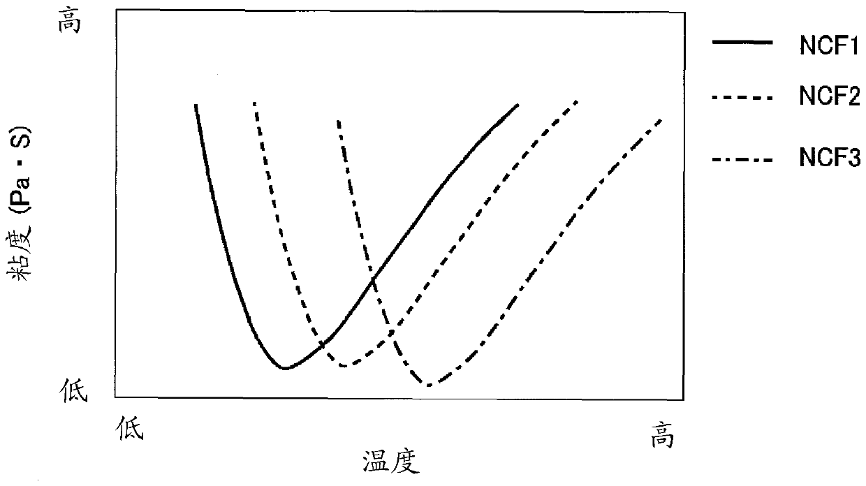
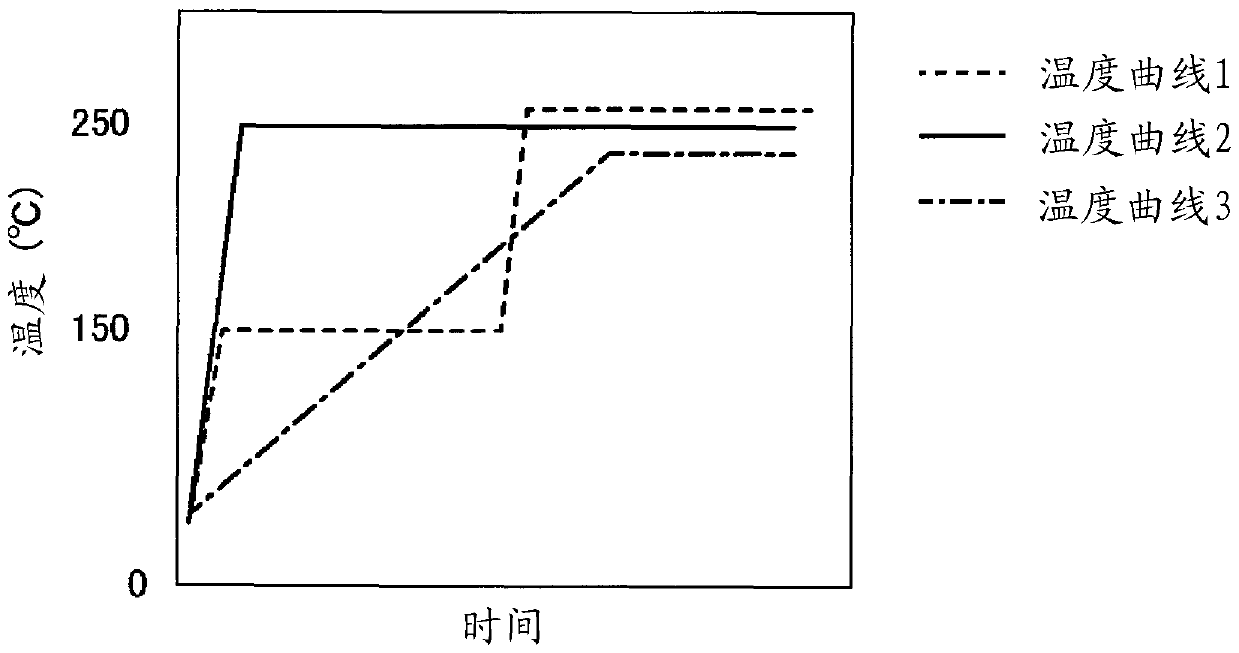
[0076] Hereinafter, examples of the present invention will be described. In this example, a pre-feed type underfill film was produced, and the melt viscosity was measured under conditions of a temperature increase rate of 5° C. / min to 50° C. / min. Then, an IC chip having solder-attached electrodes was connected to an IC substrate having electrodes opposed thereto using an underfill film to produce a package, and voids and solder joints were evaluated. In addition, this invention is not limited to these Examples.
[0077] The measurement of the melt viscosity, the preparation of the package, the evaluation of the voids, and the evaluation of the solder joint were performed as follows.
[0078] [Measurement of Melt Viscosity]
[0079] For each underfill film, using a rheometer (ARES manufactured by TA Co., Ltd.), conditions A at 5°C / min and 1 Hz, condition B at 10°C / min and 1 Hz, condition C at 20°C / min and 1 Hz, and 30 Under condition D of °C / min, 1 Hz, condition E...
PUM
Property
Measurement
Unit
melting point
aaaaa
aaaaa
melting point
aaaaa
aaaaa
melting point
aaaaa
aaaaa
Abstract
Provided are an underfill material capable of realizing a wide mounting margin, and a method of manufacturing a semiconductor device using the same. The minimum melting point when measuring the melt viscosity at a heating rate of 5°C / min to 50°C / min using an underfill material (20) containing epoxy resin, acid anhydride, acrylic resin, and organic peroxide The viscosity attainment temperature is not less than 100°C and not more than 150°C, and the minimum melt viscosity is not less than 100 Pa·s and not more than 5000 Pa·s. Since the change in the temperature at which the minimum melt viscosity is measured under different heating temperature conditions is small, even if the temperature profile at the time of thermocompression bonding is not strictly controlled, it is possible to achieve no-gap mounting and good solder joint performance, and it is possible to realize a wide the mounting edge.
Description
technical field [0001] The present invention relates to an underfill material for mounting a semiconductor chip, and a method of manufacturing a semiconductor device using the same. This application claims priority based on Japanese Patent Application No. Japanese Patent Application No. 2013-188683 for which it applied in Japan on September 11, 2013, and takes in this application by referring this application. Background technique [0002] In recent years, in semiconductor chip mounting methods, the use of "pre-applied underfill film (PUF: Pre-applied Underfill Film)" in which an underfill film is pasted on semiconductor IC (Integrated Circuit) electrodes has been studied in order to shorten the process. [0003] A mounting method using this pre-feed type underfill film is performed, for example, as follows (for example, refer to Patent Document 1). [0004] Step A: An underfill film is pasted on a wafer, followed by dicing to obtain semiconductor chips. [0005] Step B: A...
Claims
Application Information
Patent Timeline
Application Date:The date an application was filed.
Publication Date:The date a patent or application was officially published.
First Publication Date:The earliest publication date of a patent with the same application number.
Issue Date:Publication date of the patent grant document.
PCT Entry Date:The Entry date of PCT National Phase.
Estimated Expiry Date:The statutory expiry date of a patent right according to the Patent Law, and it is the longest term of protection that the patent right can achieve without the termination of the patent right due to other reasons(Term extension factor has been taken into account ).
Invalid Date:Actual expiry date is based on effective date or publication date of legal transaction data of invalid patent.
