Underfill material and process for producing semiconductor device using same

An underfill material and semiconductor technology, which is applied in semiconductor/solid-state device manufacturing, semiconductor devices, semiconductor/solid-state device components, etc., can solve the problem of narrow mounting edge, achieve wide mounting edge, good solder joint performance, The effect of gap installation

Active Publication Date: 2016-04-20
DEXERIALS CORP
View PDF10 Cites 2 Cited by
  • Summary
  • Abstract
  • Description
  • Claims
  • Application Information

AI Technical Summary

Problems solved by technology

Also, the underfill material only fits well with generally defined installation curves, the installation edge ( )narrow

Method used


Image

  • Underfill material and process for producing semiconductor device using same
  • Underfill material and process for producing semiconductor device using same
  • Underfill material and process for producing semiconductor device using same

Examples


Embodiment approach

[0071] In addition, this technology can also be applied to TSV (Through Silicon Via) technology that electrically connects a plurality of chip substrates stacked in a sandwich shape by filling metal into small holes provided in a semiconductor chip.

[0072] That is, it can also be applied to a method of manufacturing a semiconductor device in which a plurality of chip substrates having a first surface on which electrodes with solder are formed and a second surface on which a plurality of chip substrates are stacked are formed on the first surface. On the opposite side, a counter electrode opposite to the electrode with solder is formed.

[0073] At this time, the underfill film is mounted on the second surface of the second chip substrate with the underfill film attached to the first surface side of the first chip substrate. Thereafter, by thermocompression-bonding the first surface of the first chip substrate and the second surface of the second chip substrate at a temperatu...

Embodiment

[0075]

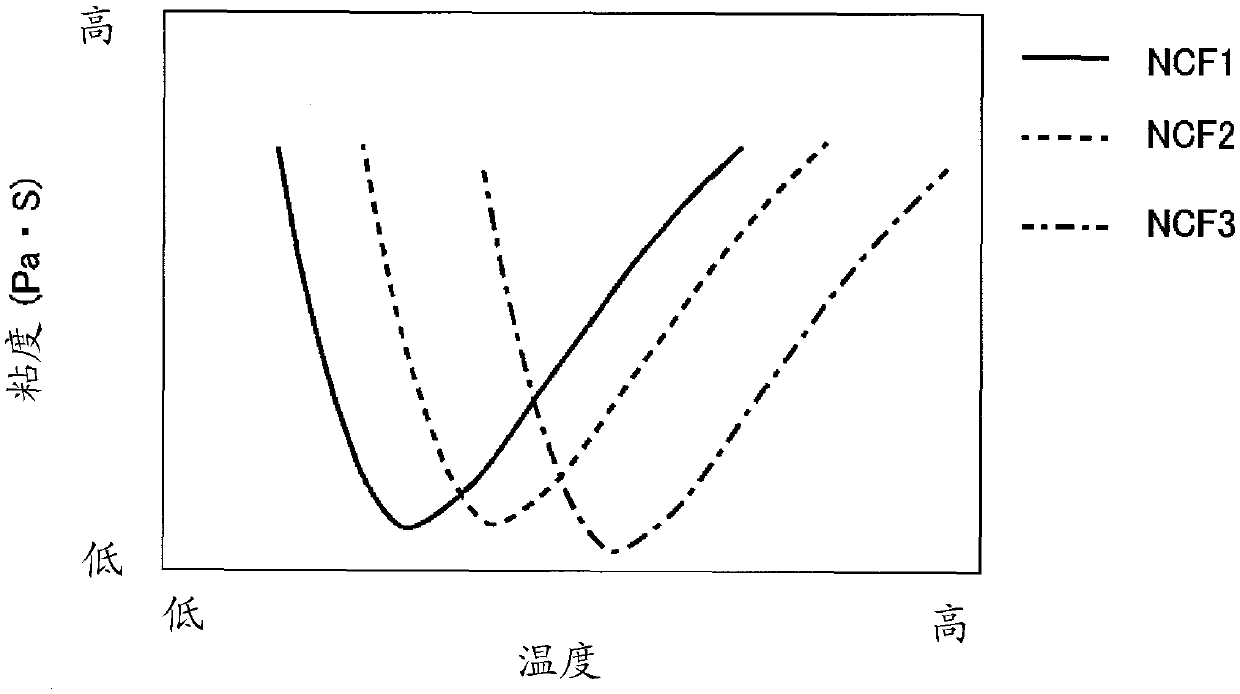
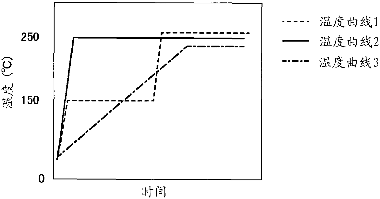
[0076] Hereinafter, examples of the present invention will be described. In this example, a pre-feed type underfill film was produced, and the melt viscosity was measured under conditions of a temperature increase rate of 5° C. / min to 50° C. / min. Then, an IC chip having solder-attached electrodes was connected to an IC substrate having electrodes opposed thereto using an underfill film to produce a package, and voids and solder joints were evaluated. In addition, this invention is not limited to these Examples.

[0077] The measurement of the melt viscosity, the preparation of the package, the evaluation of the voids, and the evaluation of the solder joint were performed as follows.

[0078] [Measurement of Melt Viscosity]

[0079] For each underfill film, using a rheometer (ARES manufactured by TA Co., Ltd.), conditions A at 5°C / min and 1 Hz, condition B at 10°C / min and 1 Hz, condition C at 20°C / min and 1 Hz, and 30 Under condition D of °C / min, 1 Hz, condition E...


PUM

PropertyMeasurementUnit
melting pointaaaaaaaaaa

Abstract

Provided are: an underfill material which enables a wide mounting margin; and a process for producing a semiconductor device using the same. This underfill material (20) comprises an epoxy resin, an acid anhydride, an acrylic resin and an organic peroxide, and exhibits a lowest-melt-viscosity reaching temperature of 100 to 150 DEG C and a lowest melt viscosity of 100 to 5000Pa s as determined under temperature rise conditions of 5 to 50 DEG C/min. Since the lowest-melt-viscosity reaching temperature of the underfill material varies only slightly as measured under various temperature rise conditions, the underfill material can ensure void-less mounting and good solder jointing even when the temperature profile in thermocompression bonding is not strictly controlled, thus enabling a wide mounting margin.

Description

technical field [0001] The present invention relates to an underfill material for mounting a semiconductor chip, and a method of manufacturing a semiconductor device using the same. This application claims priority based on Japanese Patent Application No. Japanese Patent Application No. 2013-188683 for which it applied in Japan on September 11, 2013, and takes in this application by referring this application. Background technique [0002] In recent years, in semiconductor chip mounting methods, the use of "pre-applied underfill film (PUF: Pre-applied Underfill Film)" in which an underfill film is pasted on semiconductor IC (Integrated Circuit) electrodes has been studied in order to shorten the process. [0003] A mounting method using this pre-feed type underfill film is performed, for example, as follows (for example, refer to Patent Document 1). [0004] Step A: An underfill film is pasted on a wafer, followed by dicing to obtain semiconductor chips. [0005] Step B: A...

Claims


Application Information

Patent Timeline
Patent Type & Authority Applications(China)
IPC IPC(8): H01L21/60C09J7/00C09J11/06C09J133/04C09J163/08
CPCC09J133/04C09J163/08H01L21/6836H01L2221/68327H01L2221/68377H01L2224/73104H01L2224/83191H01L2224/271H01L23/293H01L21/563H01L24/13H01L24/16H01L24/27H01L24/29H01L24/32H01L24/73H01L24/81H01L24/83H01L24/92H01L24/94H01L25/0657H01L25/50H01L2224/13025H01L2224/13111H01L2224/13147H01L2224/16146H01L2224/16227H01L2224/16238H01L2224/2919H01L2224/29191H01L2224/2929H01L2224/29291H01L2224/29387H01L2224/32145H01L2224/32225H01L2224/81191H01L2224/81204H01L2224/81444H01L2224/81815H01L2224/83204H01L2224/83862H01L2224/92H01L2224/9211H01L2224/9212H01L2224/94H01L2225/06517H01L2224/27003H01L2225/06513C09D133/066C09J133/066C08G59/42C08L63/00C09D163/00H01L2924/01082H01L2924/01083H01L2924/01047H01L2924/01029H01L2924/01051H01L2924/00014H01L2924/00012H01L2924/0665H01L2924/0635H01L2924/05442H01L2924/05341H01L2924/0549H01L2924/0532H01L2924/0102H01L2924/0544H01L2924/01006H01L2924/01012H01L2224/27H01L2224/81H01L2224/83H01L2224/11H01L21/78C08K5/14C08L33/10H01L23/3142
Inventor 斋藤崇之小山太一森山浩伸
Owner DEXERIALS CORP
Why Eureka
Try Eureka