Underfill material and method for manufacturing semiconductor device using same

An underfill material and semiconductor technology, applied in semiconductor/solid-state device manufacturing, semiconductor devices, semiconductor/solid-state device components, etc., can solve the problems of non-Bingham fluidity, insufficient air removal, etc., and achieve good performance Effect of Solder Bondability

Active Publication Date: 2016-01-27
DEXERIALS CORP
View PDF10 Cites 4 Cited by
  • Summary
  • Abstract
  • Description
  • Claims
  • Application Information

AI Technical Summary

Problems solved by technology

For example, the storage elastic modulus G' is usually set below 10E+04Pa, and the loss elastic modulus G" is set at about 10E+03Pa, and the fluidity in the molten state does not show non-Bingham fluidity, so the removal of air during installation is insufficient. Become a mounted body with voids inside

Method used


Image

  • Underfill material and method for manufacturing semiconductor device using same
  • Underfill material and method for manufacturing semiconductor device using same
  • Underfill material and method for manufacturing semiconductor device using same

Examples


Embodiment approach

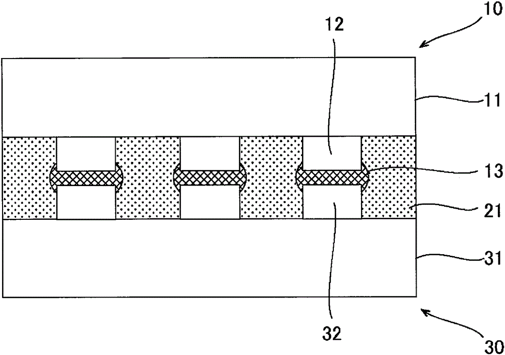
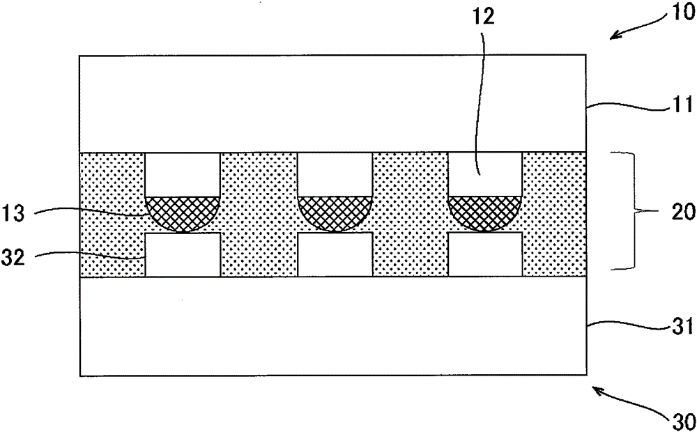
[0067] In addition, this technology can also be applied to TSV (Through Silicon Via: Through Silicon Via) technology that electrically connects a plurality of chip substrates stacked in a sandwich shape by filling small holes provided in a semiconductor chip with metal.

[0068] That is, it can also be applied to a semiconductor device in which a plurality of chip substrates are stacked having a first surface on which an electrode with solder is formed and a second surface on which a counter electrode opposite to the electrode with solder is formed on the opposite side of the first surface. Manufacturing method.

[0069] In this case, the underfill film is mounted on the second surface of the second chip substrate with the underfill film attached to the first surface side of the first chip substrate. Then, the first surface of the first chip substrate and the second surface of the second chip substrate are thermocompression bonded at a temperature equal to or higher than the m...

Embodiment

[0071]

[0072] Hereinafter, examples of the present invention will be described. In this example, a pre-feed type underfill film was produced, and the dynamic viscoelasticity measurement was performed. Then, an IC chip having electrodes with solder and an IC substrate having electrodes opposed thereto were connected to each other using an underfill film to produce a package, and voids and solder joint states were evaluated. In addition, this invention is not limited to these Examples.

[0073] The dynamic viscoelasticity measurement, fabrication of the package, evaluation of voids, and evaluation of solder joints were performed as follows.


PUM

PropertyMeasurementUnit
melting pointaaaaaaaaaa

Abstract

This invention provides: an underfill material that allows void-free mounting and good soldering performance; and a method for manufacturing a semiconductor device using said underfill material. Said underfill material contains an epoxy resin, an acid anhydride, an acrylic resin, and an organic peroxide and exhibits non-Bingham fluidity at a temperature between 60 DEG C and 100 DEG C, inclusive. The storage modulus (G') of said underfill material as per dynamic viscoelastic measurement has an inflection point at an angular frequency less than or equal to 102 rad/s, and at angular frequencies less than or equal to said inflection point, the storage modulus (G') falls between 105 and 106 Pa, inclusive. The use of said underfill material allows void-free mounting and good soldering performance.

Description

technical field [0001] The present invention relates to an underfill material used for mounting a semiconductor chip and a method of manufacturing a semiconductor device using the underfill material. This application claims priority on the basis of Japanese Patent Application No. Japanese Patent Application No. 2013-187980 for which it applied in Japan on September 11, 2013, By referring this application, this application is used here. Background technique [0002] In recent years, in the semiconductor chip mounting method, for the purpose of shortening the process, the "pre-applied underfill film (PUF: Pre-applied Underfill Film)" that pastes the underfill film on the electrode of the semiconductor IC (Integrated Circuit, integrated circuit) has been studied. use. [0003] The mounting method using this pre-feed type underfill film is performed, for example, as follows (for example, refer to Patent Document 1). [0004] Step A: The underfill film is pasted on the wafer an...

Claims


Application Information

Patent Timeline
Patent Type & Authority Applications(China)
IPC IPC(8): H01L21/60C09J7/00C09J11/06C09J133/16C09J163/02
CPCH01L21/6836H01L2221/68327H01L2221/68377H01L2224/73104H01L2224/83191H01L2224/271H01L23/293H01L21/563H01L24/13H01L24/16H01L24/27H01L24/29H01L24/32H01L24/73H01L24/81H01L24/83H01L24/92H01L24/94H01L25/0657H01L25/50H01L2224/13025H01L2224/13111H01L2224/13147H01L2224/16146H01L2224/16227H01L2224/16238H01L2224/2919H01L2224/29191H01L2224/2929H01L2224/29291H01L2224/29387H01L2224/32145H01L2224/32225H01L2224/81191H01L2224/81204H01L2224/81815H01L2224/83204H01L2224/83862H01L2224/92H01L2224/9211H01L2224/9212H01L2224/94H01L2225/06517H01L2224/27003H01L2225/06513C09D133/066C08G59/4215C08L63/00H01L2924/01082H01L2924/01083H01L2924/01047H01L2924/01029H01L2924/01051H01L2924/00014H01L2924/00012H01L2924/0665H01L2924/0635H01L2924/05442H01L2924/05341H01L2924/0549H01L2924/0532H01L2924/0102H01L2924/0544H01L2924/01006H01L2924/01012H01L2224/27H01L2224/81H01L2224/83H01L2224/11H01L21/78C08L33/16C09J7/00C09J133/20C09J163/00C09J2203/326C09J2301/312H01L2224/81193H01L2224/81203H01L2924/186
Inventor 小山太一
Owner DEXERIALS CORP
Why Eureka
Try Eureka