Chip surface contact pressure calculation method and variable-scale manufacturability design method

A technology of contact pressure and calculation method, which is applied in calculation, instrumentation, electrical digital data processing, etc., and can solve problems such as lack of CMP model realization technology

Active Publication Date: 2016-06-01
INST OF MICROELECTRONICS CHINESE ACAD OF SCI
View PDF4 Cites 1 Cited by
  • Summary
  • Abstract
  • Description
  • Claims
  • Application Information

AI Technical Summary

Problems solved by technology

[0004] However, in the prior art, the CMP model and implementation technology that can take into account both the grinding mechanism and the calculation efficiency of the contact pressure between the polishing pad and the chip surface are very scarce, res...

Method used


Image

  • Chip surface contact pressure calculation method and variable-scale manufacturability design method
  • Chip surface contact pressure calculation method and variable-scale manufacturability design method
  • Chip surface contact pressure calculation method and variable-scale manufacturability design method

Examples


Embodiment Construction

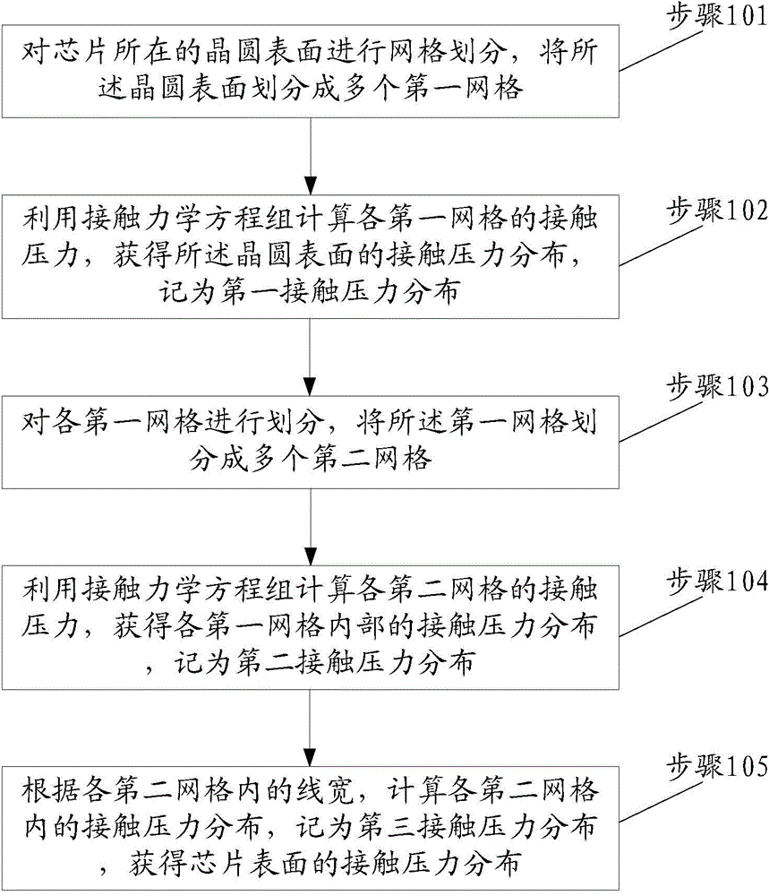
[0059] As mentioned in the background technology section, in the prior art, the CMP model and implementation technology that can take into account both the grinding mechanism and the calculation efficiency of the contact pressure between the polishing pad and the surface of the chip are very scarce, resulting in a polishing pad and chip that can take into account both calculation efficiency and accuracy. The research on the calculation method of contact pressure between surfaces has become an important topic in the process of CMP dynamic simulation.

[0060] The inventor found that in recent years, CMP theory and simulation research have promoted the application of CMP models in process simulation and design optimization, but there are not many chip-level CMP models that are actually adopted by design companies and developed into products. The geometric semi-empirical models of Provincial Institute of Technology and Berkeley are the main ones. This is mainly because there are ...


PUM


Abstract

The invention discloses a chip surface contact pressure calculation method and a variable-scale manufacturability design method. The calculation method comprises the steps of performing grid division on a wafer surface where a chip is to obtain a plurality of first grids; calculating a contact pressure of each first grid by utilizing a contact mechanical equation set to obtain contact pressure distribution of the wafer surface, and marking the contact pressure distribution as first contact pressure distribution; dividing each first grid into a plurality of second grids; calculating a contact pressure of each second grid by utilizing the contact mechanical equation set to obtain contact pressure distribution in each first grid, and marking the contact pressure distribution as second contact pressure distribution; and according to the line width in each second grid, calculating contact pressure distribution in each second grid, marking the contact pressure distribution as third contact pressure distribution, and obtaining contact pressure distribution of the chip surface. According to the chip surface contact pressure calculation method provided by the invention, the calculation efficiency and the calculation precision can be considered simultaneously, thereby providing premise and guarantee for manufacturability design optimization.

Description

technical field [0001] The invention relates to the field of manufacturability design of integrated circuits, in particular to a method for calculating chip surface contact pressure and a method for manufacturability design with variable scale. Background technique [0002] In recent years, with the continuous expansion of integrated circuit wafer size and the continuous reduction of chip feature size, chip stability control has become increasingly difficult. Many derivative effects have not been fully considered before design, and the improvement of integrated circuit yield has been significantly affected. Therefore, the IC chip design process solution based on Design for Manufacturability (DFM) has become a frontier research hotspot in recent years. Design for Manufacturability (DFM), as a nascent nano-design methodology technology, provides a technical platform covering design and manufacturing information, so that designers can predict the impact of different design sche...

Claims


Application Information

Patent Timeline
IPC IPC(8): G06F17/50
Inventor 徐勤志陈岚
Owner INST OF MICROELECTRONICS CHINESE ACAD OF SCI
Why Eureka
Try Eureka