Pixel circuit, driving method for the same, display panel

A technology of pixel circuit and power supply terminal, which is applied in the direction of static indicators, instruments, etc., can solve the problems of limiting the application range of MIP display technology, complex circuit structure, and difficult implementation, so as to achieve the effect of static display

Active Publication Date: 2016-06-01
BOE TECH GRP CO LTD +1
View PDF8 Cites 14 Cited by
  • Summary
  • Abstract
  • Description
  • Claims
  • Application Information

AI Technical Summary

Problems solved by technology

[0004] However, due to the complex circuit structure of the existing analog voltage storage unit, it is difficult to integrate it into the pixel circuit. Therefore, most of the prior art uses integrated 1Bit digital memor

Method used


Image

  • Pixel circuit, driving method for the same, display panel
  • Pixel circuit, driving method for the same, display panel
  • Pixel circuit, driving method for the same, display panel

Examples


Embodiment 1

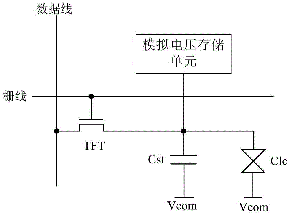
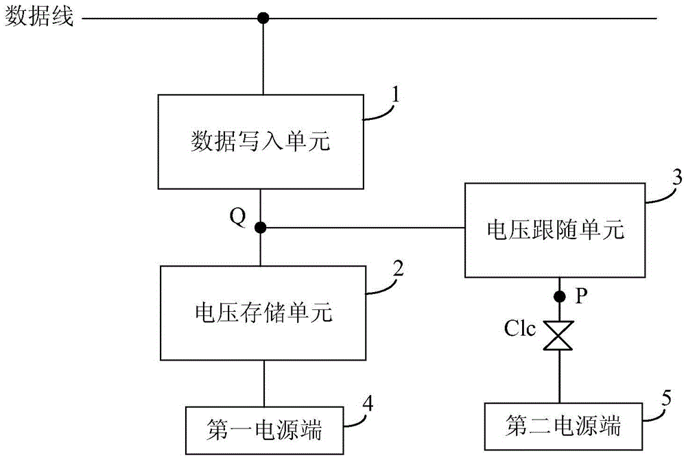
[0064] figure 2 A schematic circuit diagram of a pixel circuit provided in Embodiment 1 of the present invention, such as figure 2 As shown, the pixel circuit includes two working modes: normal display mode and static display mode, and the pixel circuit includes: data writing unit 1, voltage storage unit 2, voltage following unit 3 and liquid crystal capacitor Clc.

[0065] Wherein, the data writing unit 1 is connected with the voltage storage unit 2 and the voltage following unit 3, and the data writing unit 1 is used to send the data voltage on the data line to the voltage storage unit 2 and the voltage follower unit 3 when the pixel circuit is in the normal display mode. Follow Unit 3.

[0066] The voltage storage unit 2 is connected to the first power supply terminal 4 and the input terminal of the voltage follower unit 3, the voltage storage unit 2 is used to store the data voltage when the pixel circuit is in the normal display mode, and when the pixel circuit is in t...

Embodiment 2

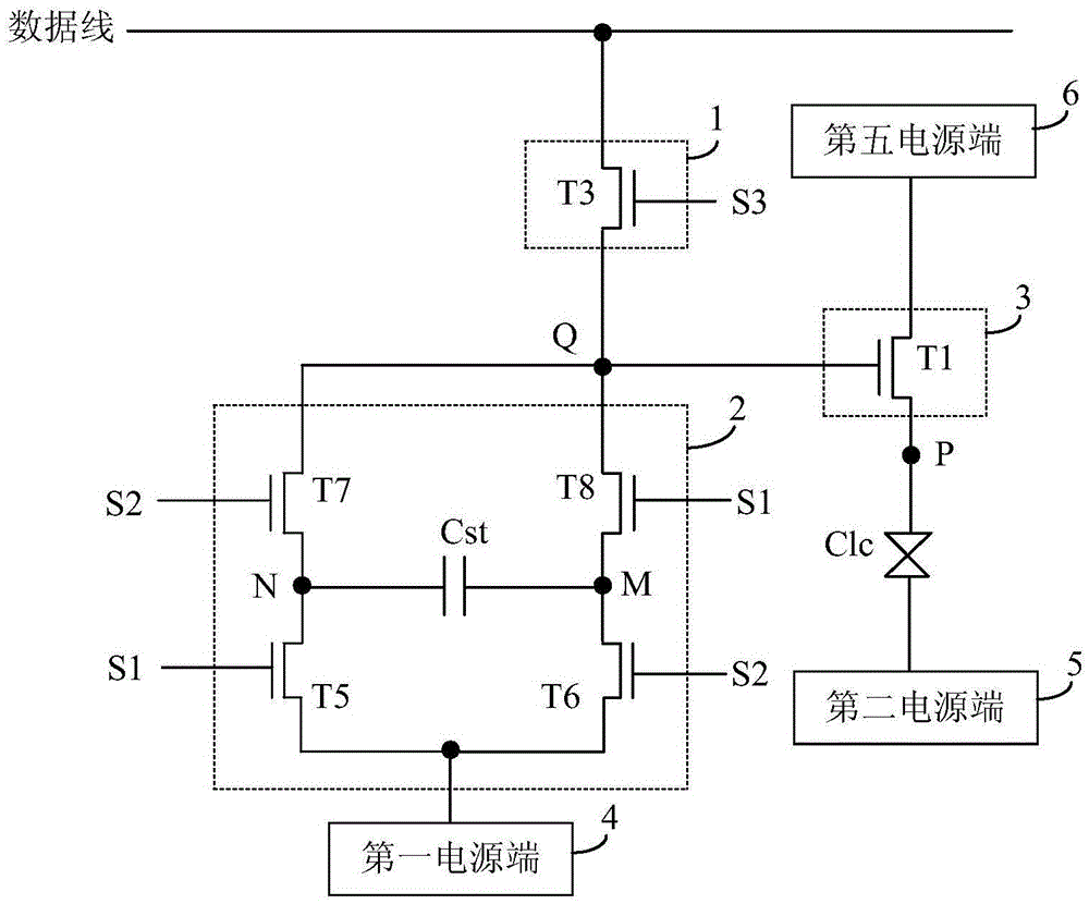
[0088] image 3 A schematic circuit diagram of a pixel circuit provided in Embodiment 2 of the present invention, such as image 3 as shown, image 3 The pixel circuit shown is based on figure 2 A specific scheme of the pixel circuit shown.

[0089] Optionally, the data writing unit 1 includes: a third transistor T3. Wherein, the control electrode of the third transistor T3 is connected to the third control line S3, the first electrode of the third transistor T3 is connected to the data line, the second electrode of the third transistor T3 is connected to the input terminal of the voltage follower unit 3 and the voltage storage unit 2 connections.

[0090] Optionally, the voltage following unit 3 includes: a first transistor T1. Wherein, the first transistor T1 is a common-drain amplifier transistor, the gate of the first transistor T1 is connected to the data writing unit 1 and the voltage storage unit 2, the source of the first transistor T1 is connected to the fifth p...

Embodiment 3

[0115] Embodiment 3 of the present invention provides a pixel circuit, which is based on figure 2 A modification of the pixel circuit shown.

[0116] exist figure 2 In the actual working process of the pixel circuit shown, the pixel circuit cannot maintain a static display for a long time. figure 2 The principle why the pixel circuit shown cannot maintain a static display for a long time is explained in detail. Wherein, it is assumed that the data voltage Vdata on the data line is greater than the voltage Vref of the first power terminal 4 .

[0117] when figure 2 When the pixel circuit shown is in the second stage, although the sixth transistor T6 is in the cut-off state, since the first pole of the sixth transistor T6 is connected to the first power supply terminal 4, the second phase between the first power supply terminal 4 and the storage capacitor Cst A leakage current (a small current flowing through the sixth transistor T6) is easily generated between terminals...


PUM


Abstract

The invention discloses a pixel circuit, a driving method for the same and a display panel. The pixel circuit comprises a data writing-in unit, a voltage storage unit, a voltage following unit and a liquid crystal capacitor, wherein the data writing-in unit is used for transmitting data voltage on the data line to the voltage storage unit and the voltage following unit when the pixel circuit is in the normal display module mode; the voltage storage unit is used for storing the data voltage when the pixel circuit is in the normal display mode and transmitting the data voltage or regulation voltage to the input terminal of the voltage following unit when the pixel circuit is in the static display mode; the voltage following unit is used for outputting corresponding data output voltage according to the data voltage provided by the voltage storage unit or the regulation voltage in order to allow the liquid crystal capacitor to generate a corresponding liquid crystal deflecting electric field. The technical field of the invention can realize the static display of the color image by the display panel.

Description

technical field [0001] The invention relates to the field of display technology, in particular to a pixel circuit, a driving method thereof, and a display panel. Background technique [0002] With the development of technologies such as smart wear and mobile applications, there are requirements for the development of ultra-low power LCD display technology. Memory in Pixel (MIP) display technology, as a new type of low-power LCD display technology, has broad development prospects due to its characteristics of no need to change the LCD process, no need for new material development, simple structure, and low cost. [0003] figure 1 It is a schematic circuit diagram of a pixel driving circuit in the prior art, such as figure 1 As shown, the pixel drive circuit includes: a switching transistor TFT, an analog voltage storage unit (AnalogMemoryUint), a storage capacitor Cst and a liquid crystal capacitor Clc, when the display panel is in a standby state or displays a static pictu...

Claims


Application Information

Patent Timeline
IPC IPC(8): G09G3/36
CPCG09G3/36G09G3/3648G09G2310/08G09G2320/103G09G2330/021G09G3/3614G09G2300/0823G09G2300/0842G09G2320/0214G09G3/3651G09G2300/0452G09G2300/0482G09G2320/0204G09G2320/0242G09G2320/0295
Inventor 谭文陈佳
Owner BOE TECH GRP CO LTD
Why Eureka
Try Eureka