Integrated circuit manufacturing methods

A technology of integrated circuit and manufacturing method, which is applied in the direction of circuit, semiconductor/solid-state device manufacturing, electrical components, etc., and can solve problems such as high cost and complicated process

Inactive Publication Date: 2016-06-01
CSMC TECH FAB2 CO LTD
View PDF5 Cites 0 Cited by
  • Summary
  • Abstract
  • Description
  • Claims
  • Application Information

AI Technical Summary

Problems solved by technology

[0004] None of the above methods can directly integrate high-voltage components in general-purpose medium and low-voltage integrated circuits to achieve step-down processing, which has the disadvantages of complex process and high cost

Method used


Image

  • Integrated circuit manufacturing methods
  • Integrated circuit manufacturing methods
  • Integrated circuit manufacturing methods

Examples


Embodiment Construction

[0078] The present invention provides three different integrated circuit manufacturing methods, which will be described below in conjunction with specific drawings and corresponding embodiments.

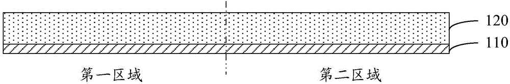
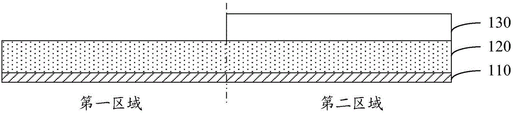
[0079] Please refer to figure 1 and Figure 2-7 , is a flowchart of the first integrated circuit manufacturing method in an embodiment and a schematic diagram of corresponding effects.

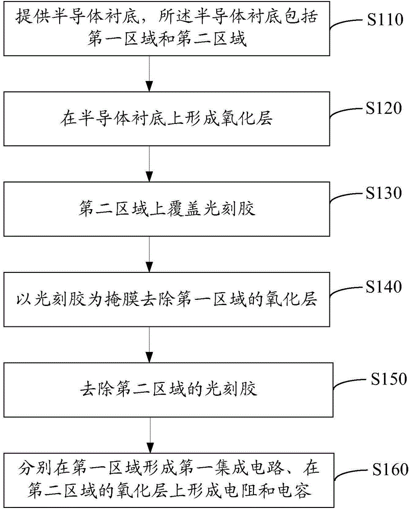
[0080] Step S110: providing a semiconductor substrate, the semiconductor substrate including a first region and a second region.

[0081] In this embodiment, the semiconductor substrate 110 can be either N-type or P-type. The first area here is used to form the first integrated circuit, and the voltage capability of the first integrated circuit is below 250 volts, so the first area is also called the medium and low voltage area, and the first integrated circuit is also called the medium and low voltage integrated circuit. The second area here is used to form resistors and capacitors, which can wit...


PUM


Abstract

An integrated circuit manufacturing method comprises the steps of: providing a semiconductor substrate, wherein the semiconductor substrate comprises a first area and a second area; forming an oxide layer on the semiconductor substrate; covering the second area with a photoresist; using the photoresist as a mask to remove the oxide layer in the first layer; removing the photoresist in the second area; respectively forming a first integrated circuit in the first area and forming a resistor and a capacitor on the oxide layer of the second area. The invention further provides the other two integrated circuit manufacturing methods. According to the invention, the technology is simple, the cost is low, the resistor and capacitor in the second area can be more conveniently integrated with the integrated circuit in the first area, in addition, the original characteristics of the integrated circuit in the first area are not changed.

Description

technical field [0001] The invention relates to the field of manufacturing integrated circuits, in particular to a method for manufacturing integrated circuits. Background technique [0002] The voltage range of the high-voltage direct current is between 110 volts and 400 volts, and the power supply voltage of the primary side power management chip generally does not exceed 40 volts. Therefore, the high-voltage direct current voltage cannot directly supply power to the primary-side power management chip, and additional high-voltage components (such as high-voltage resistors or capacitors) are required to step down the high-voltage direct current voltage. [0003] There are three existing voltage reduction methods: the first is to configure discrete high-voltage resistors or discrete capacitors above 400 volts on the circuit board around the chip; the second is to use multi-chip packaging technology to integrate discrete high-voltage Resistive or discrete capacitive componen...

Claims


Application Information

Patent Timeline
Patent Type & Authority Applications(China)
IPC IPC(8): H01L21/82
Inventor 张森
Owner CSMC TECH FAB2 CO LTD
Why Eureka
Try Eureka