GaN growth method based on graphene and magnetron sputtering AlN

A magnetron sputtering and growth method technology, applied in the field of electronics, can solve the problems of poor quality of nitride materials, high growth temperature, and high temperature of nitride materials, and achieve the effect of improving material quality and improving quality

Active Publication Date: 2019-01-29
XIDIAN UNIV
View PDF4 Cites 0 Cited by
  • Summary
  • Abstract
  • Description
  • Claims
  • Application Information

AI Technical Summary

Problems solved by technology

But, the weak point that this method still exists is: 1, because this method is to carry out epitaxy on copper substrate, make the nitride material temperature of follow-up growth can not be higher than the melting point of copper
As aluminum nitride is commonly used as a nucleation layer, its suitable growth temperature is higher than the melting point, so this method cannot grow a good AlN layer, which makes the quality of the obtained nitride material poor.
2. This method lacks a transition layer and can only grow nitride materials on substrates with small lattice mismatches

Method used


Image

  • GaN growth method based on graphene and magnetron sputtering AlN
  • GaN growth method based on graphene and magnetron sputtering AlN

Examples


Embodiment 1

[0050] Example 1: Ga-face gallium nitride based on graphene and magnetron sputtered aluminum nitride.

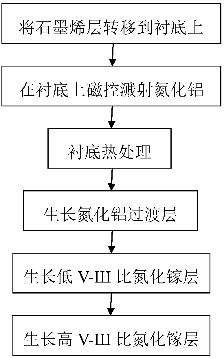
[0051] Step 1. Transfer graphene.

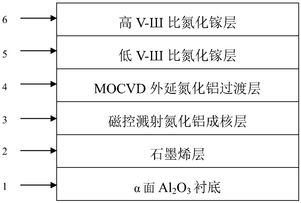
[0052] Firstly, a 0.34nm single-layer graphene is grown on a copper substrate by chemical vapor deposition. Then the monolayer graphene was placed in a mixed solution of 1M ferric chloride and 2M hydrochloric acid for 12 hours. Transfer of monolayer graphene to α-face Al after removing the copper substrate 2 o 3 On the substrate, the Al covered graphene is obtained 2 o 3 substrate.

[0053] Step 2. Magnetron sputtering aluminum nitride.

[0054] Al 2 o 3 The substrate was placed in a magnetron sputtering system, the pressure of the reaction chamber was 1Pa, and nitrogen and argon were introduced into the system for 5 minutes. Then use 5N pure aluminum as the target material, and use radio frequency magnetron sputtering 2 o 3 A 30nm aluminum nitride film was sputtered on the substrate to obtain a sputtered aluminum nitride substr...

Embodiment 2

[0064] Example 2: N-face gallium nitride based on graphene and magnetron sputtered aluminum nitride.

[0065] Step 1. Transfer graphene.

[0066] Firstly, a 0.34nm single-layer graphene is grown on a copper substrate by chemical vapor deposition. Then the monolayer graphene was placed in a mixed solution of 1M ferric chloride and 2M hydrochloric acid for 12 hours. Transfer of monolayer graphene to α-face Al after removing the copper substrate 2 o 3 On the substrate, the Al covered graphene is obtained 2 o 3 substrate.

[0067] Step 2. Magnetron sputtering aluminum nitride.

[0068] Al 2 o 3 The substrate was placed in a magnetron sputtering system, the pressure of the reaction chamber was 1Pa, and nitrogen and argon were introduced into the system for 5 minutes. Then use 5N pure aluminum as the target material, and use radio frequency magnetron sputtering 2 o 3 A 80nm aluminum nitride thin film is sputtered on the substrate to obtain a sputtered aluminum nitride sub...


PUM

PropertyMeasurementUnit
thicknessaaaaaaaaaa
thicknessaaaaaaaaaa
thicknessaaaaaaaaaa

Abstract

The invention discloses a gallium nitride growth method based on graphene and magnetron sputtering aluminum nitride. The gallium nitride growth method is mainly used for improving the material quality of gallium nitride. The gallium nitride growth method comprises the following growth steps: (1) transferring a layer of graphene on a sapphire substrate; (2) carrying out magnetron sputtering on an aluminum nitride nucleating layer on the graphene; (3) carrying out heat treatment on the surface; (4) growing an aluminum nitride transition layer; (5) growing a gallium nitride layer with low V-III ratio; and (6) growing a gallium nitride layer with high V-III ratio. The gallium nitride disclosed by the invention has the advantages that graphene and magnetron sputtering aluminum nitride are combined, the gallium nitride has the advantages of good material quality and large substrate application range, and the gallium nitride can be used for manufacturing gallium nitride epitaxial layers and devices.

Description

technical field [0001] The invention belongs to the field of electronic technology, and further relates to a gallium nitride growth method based on graphene and magnetron sputtering aluminum nitride in the field of microelectronic technology. The invention can be used for making gallium nitride and its devices. Background technique [0002] The third-generation wide-bandgap semiconductor materials represented by gallium nitride are widely used in the fields of optoelectronic devices and electronic devices due to their advantages such as large bandgap width, high electron mobility, and large breakdown electric field. However, due to the large lattice mismatch and thermal mismatch between the gallium nitride material and the substrate, the gallium nitride obtained by heteroepitaxy often has a high dislocation density, and these dislocations greatly limit the nitrogen performance and reliability of GaN-based devices. Therefore, the epitaxial growth of GaN materials with low d...

Claims


Application Information

Patent Timeline
Patent Type & Authority Patents(China)
IPC IPC(8): H01L33/00H01L33/04
CPCH01L33/005H01L33/04
Inventor 张进成陈智斌吕佳骐郝跃
Owner XIDIAN UNIV
Why Eureka
Try Eureka