LED 3D display module and LED 3D display system
A display module and pixel unit technology, which can be used in stereoscopic systems, image communications, electrical components, etc., and can solve problems such as color shift and high cost of shutter-type three-dimensional display methods
- Summary
- Abstract
- Description
- Claims
- Application Information
AI Technical Summary
Problems solved by technology
Method used
Image
Examples
specific Embodiment approach 1
[0080] The manufacturing method of this embodiment comprises the following steps:
[0081] Step 1. Paste double-sided transparent tape on the LED unit board or apply a layer of transparent epoxy resin potting glue or use other types of transparent pasting materials.
[0082] Step 2. Attach a layer of protective film on the left and right circular polarizing strips to prevent the polarizing strips from being scratched or stuck to glue during the pasting process, thereby affecting the polarizing effect.
[0083] Step 3. Paste and fix the left and right circular polarizing strips alternately on the corresponding positions of the odd and even rows or columns of the LED unit board. The air bubbles are driven out.
[0084] Step 4. Peel off the protective film attached to the left and right polarizers.
[0085] Step 5. Paste a protective film or apply a layer of light-transmitting protective glue on the LED unit board on which the polarizing strip is fixed. The protective glue can ...
Embodiment approach
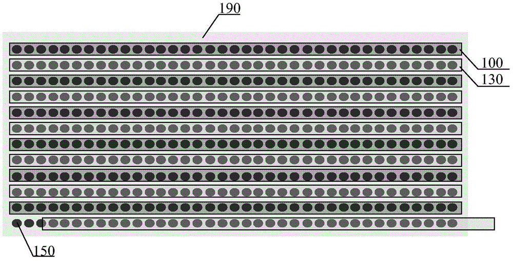
[0091] Such as Figure 9 , 10 As shown, the manufacturing method of the LED3D display module of the present invention includes: an LED display unit board 300, a plurality of left-handed and right-handed circular polarizing strips 310, 320, a driver IC50, a driver circuit board 53, an LED wafer 56, and a mask 55. The driver IC 50 is welded on the back of the driver circuit board 53 , the LED wafer 56 is fixed on the corresponding pixel position on the front of the driver circuit board 53 by SMT patches, and the mask 55 is fixed on the driver circuit board 53 and frames the LED wafer 56 . Wherein, the pixel pitch on the LED display unit board 300 is d=2mm, and the left and right circular polarizer strips 310 and 320 are respectively glued to the positions corresponding to the odd and even rows of the pixels of the LED display unit by epoxy resin. The width of the left and right circular polarizing strips 310, 320 should be greater than or equal to the width of the LED display p...
specific Embodiment approach 2
[0096] The manufacturing method of this embodiment comprises the following steps:
[0097] Step 1. Fix the mask on the LED unit board and the height of its upper surface should be between 0.1mm-1mm higher than the height of the upper surface of the LED display pixel
[0098] Step 2. Apply a layer of transparent epoxy resin potting glue or other types of transparent pasting materials on the LED unit board.
[0099] Step 3. Attach a layer of protective film on the polarizing module to prevent the polarizing module from being scratched or glued to glue during the pasting process, thereby affecting the polarizing effect.
[0100] Step 4. Paste and fix the polarizing module on the LED unit board, and the left and right polarizing strips on the polarizing module correspond to the rows or columns of the LED display pixels. Air bubbles between the display pixels are ejected on the plate.
[0101] Step 5. Peel off the protective film attached to the left and right polarizers.
[010...
PUM
 Abstract
Description
Claims
Application Information


