

A vertical GaN-based heterojunction semiconductor device and its manufacturing method
A GaN-based, manufacturing method technology, applied in semiconductor/solid-state device manufacturing, semiconductor devices, electrical components, etc., can solve the problem that the utilization rate of chip area is not as effective as that of vertical high-voltage devices, and the utilization rate of surface area is not much improved, etc. problem, to achieve the effect of simple manufacturing method, effective power, and easy realization
- Summary
- Abstract
- Description
- Claims
- Application Information
AI Technical Summary
Problems solved by technology
Method used
Image

Examples
Embodiment 1
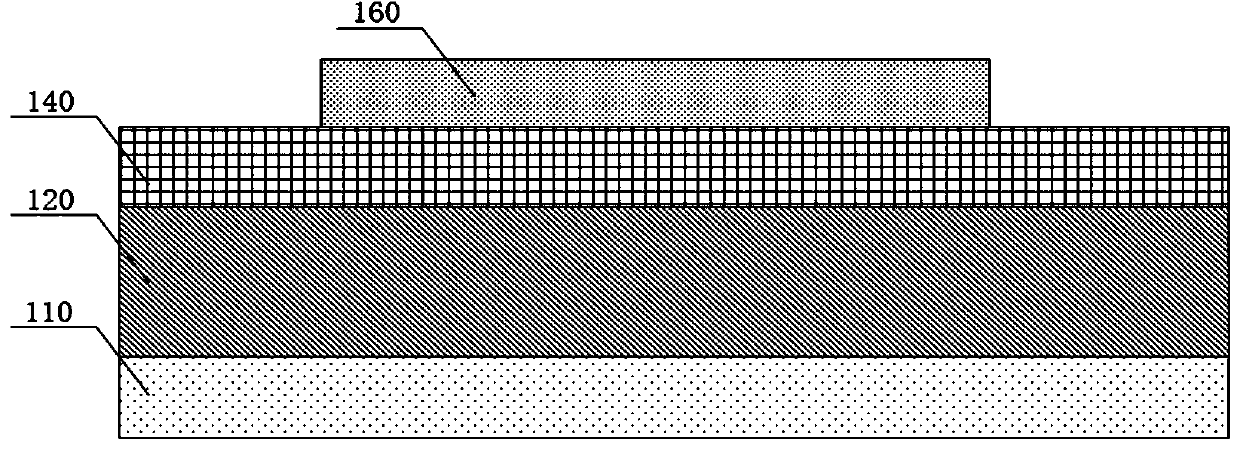
[0055] image 3 It is a front cross-sectional view of the structure of Embodiment 1 of the vertical gallium nitride-based heterojunction semiconductor device according to the present invention, such as image 3 As shown, the structure of the vertical gallium nitride-based heterojunction semiconductor device of the present invention includes a substrate 110, an unintentionally doped gallium nitride (GaN) buffer layer 120, an aluminum gallium nitride (AlGaN) barrier layer 140, and metal layer 160. An aluminum gallium nitride (AlGaN) barrier layer 140 is deposited on the longitudinal groove and surface of the unintentionally doped gallium nitride (GaN) buffer layer 120, and the unintentionally doped gallium nitride (GaN) buffer layer 120 A vertical GaN-based heterojunction is formed. The vertical GaN-based heterojunction connects the surface and the bottom surface, providing a channel for vertical current flow. The metal layer 160 is located on the surface of the vertical GaN-...
Embodiment 2
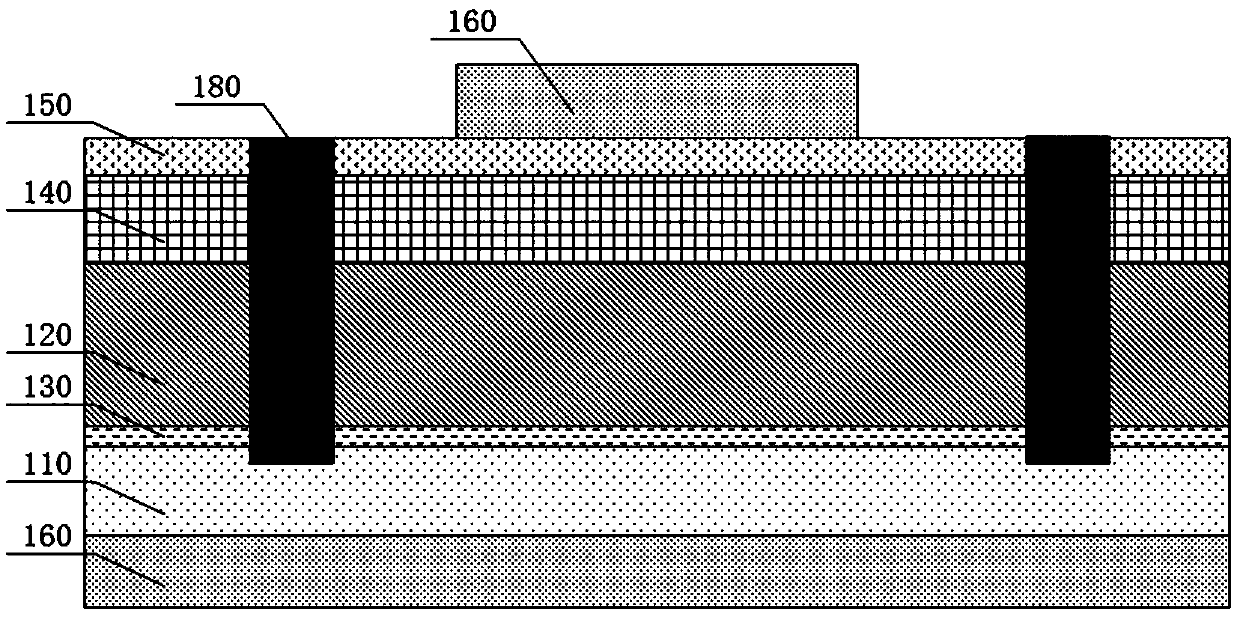
[0057] Figure 4 It is a front cross-sectional view of Embodiment 2 of a vertical gallium nitride-based heterojunction semiconductor device according to the present invention, such as Figure 4 As shown, the structure of the vertical gallium nitride-based heterojunction semiconductor device of this embodiment is similar to that of embodiment 1, except that the surface of the unintentionally doped gallium nitride (GaN) buffer layer 120 is mixed with aluminum nitrogen An N-type doped gallium nitride (GaN) layer 210 is also included between the gallium nitride (AlGaN) barrier layers 140 . The aluminum gallium nitride (AlGaN) barrier layer 140 and the unintentionally doped gallium nitride (GaN) buffer layer 120 form a vertical GaN-based heterojunction. The vertical GaN-based heterojunction connects the surface and the bottom surface, providing a channel for vertical current flow. The two-dimensional electron gas (2DEG) of the vertical gallium nitride-based heterojunction connect...
Embodiment 3
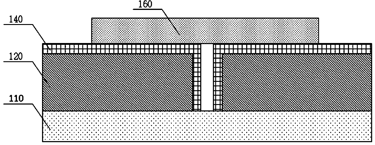
[0059] Figure 5 It is a front cross-sectional view of Embodiment 3 of a vertical gallium nitride-based heterojunction semiconductor device according to the present invention, as Figure 5 As shown, the structure of the vertical GaN-based heterojunction semiconductor device in this embodiment is similar to that in Embodiment 1, except that the aluminum gallium nitride (AlGaN) barrier layer 140 is deposited on the unintentionally doped In the vertical groove of the Gallium Nitride (GaN) buffer layer 120 . The aluminum gallium nitride (AlGaN) barrier layer 140 and the unintentionally doped gallium nitride (GaN) buffer layer 120 constitute a GaN vertical-based heterojunction and a vertical GaN-based heterojunction. The vertical GaN-based heterojunction connects the surface and the bottom surface, providing a channel for vertical current flow. The two-dimensional electron gas (2DEG) of the vertical gallium nitride-based heterojunction is connected to the metal layer 160 on the s...
PUM
| Property | Measurement | Unit |
|---|---|---|
| thickness | aaaaa | aaaaa |
| thickness | aaaaa | aaaaa |
| thickness | aaaaa | aaaaa |
Abstract
Description
Claims
Application Information